This thread has been locked.

If you have a related question, please click the "Ask a related question" button in the top right corner. The newly created question will be automatically linked to this question.

TS5A22364 Charge injection

Other Parts Discussed in Thread: TS5A22364

Dear Community,

i have used a TS5A22364 in my output path for an analog audio output. In the attachment you will find the schematic and a scope picture.

The Problem:

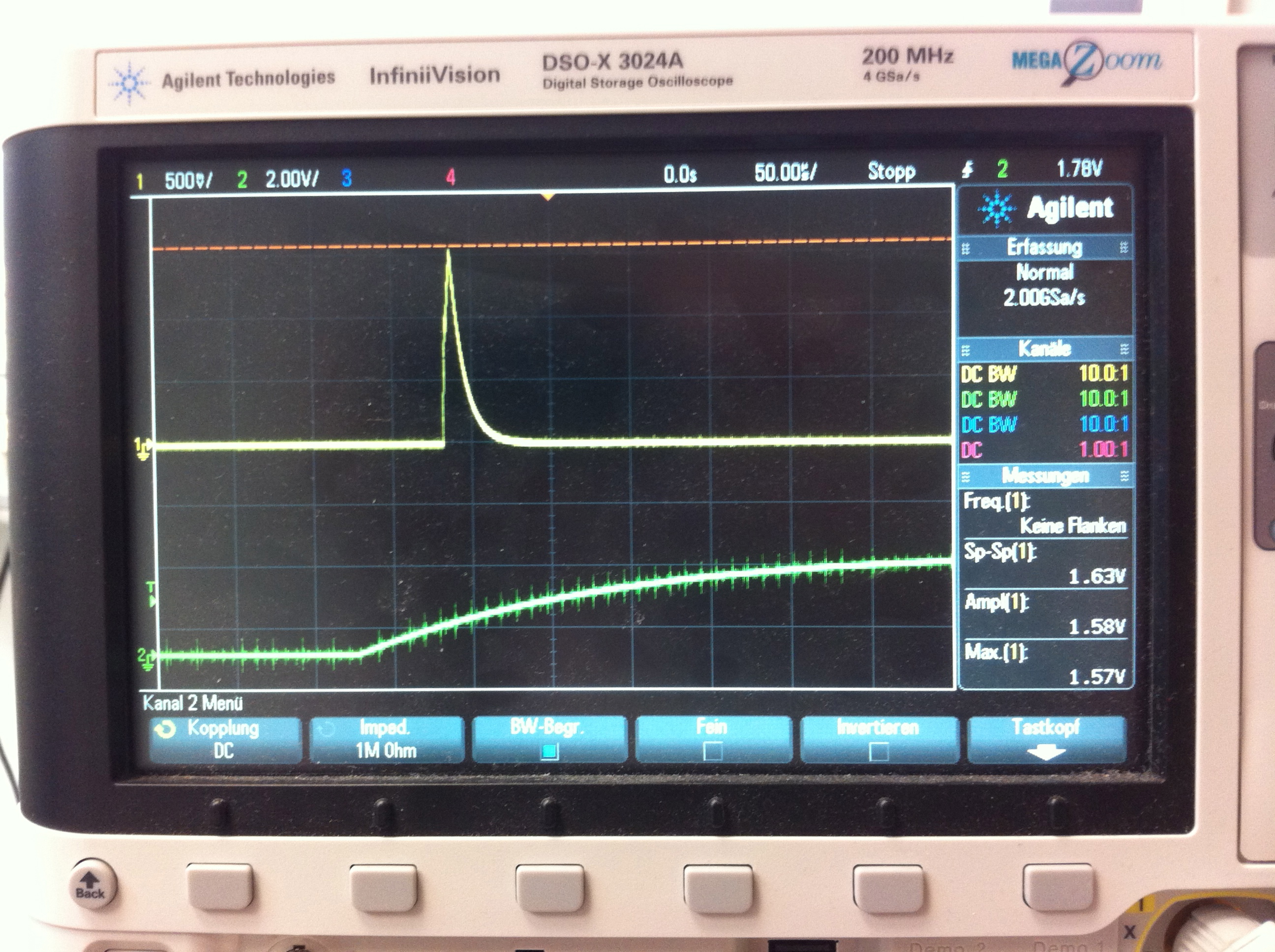
In the moment of switching the device produces an 1,5V peak on the COM and NO terminal. This peak puls is an loud audible click. I used the TS5A to prenvent the on/off click but now this devices itself produces this peak. I looked up the datasheet and there is the Charge Injection is about 150pC. Together with the output capacitator in my schematic of 10nF there should be a deltaU:

C=Q/U

U=Q/C -> 150pC / 10nF = 15mV!!! 

This could be okay.

The scope picture shows the output voltage and the control input.

I hope anybody used this switch for a similar purpose and can tell me if this peak is the normal behavior. 

Best regards,

Moritz Bente

PS: To messure the Voltage injected by the TS5A i unconnected the C17 with an without it is the same behavior.

  • Hello Moritz,

    Can you probe all three ports (NC COM and NO) at the same time?

    Also what is the condition before the pulse.  Are you switching from NO -> NC or NC -> NO?

    Can you show more of the schematic?  I would like to see where the capacitors tie off on the NO line and what the COM port connects to. 

    Regards,

    Andrew

  • I have a question regarding the application of the circuit as shown. The TS5A22364 passes a signal between Vdd and gnd. Depending on what the Vdd voltage is sets the signal swing. What is the voltage being used on the TS5A22364 in this case? If it is 5V, the signal can never swing "negative"; correct? For "full" symmetrical voltage swing Vdd should be ~+2.75V, correct?

  • Hello,

    the signals at the COM and NO port is exact the same. The Signal before the control signal rises is gnd level but

    As i mentioned before i have unsoldered the C17 to find the source of the pulse. So the pulse must be injected by the signal switch. I have no idea for another source because nothing other connected. 

    I am switching from NC -> COM to NO -> COM.

    The AVDD voltage is 3,3V so the signal on the COM terminal should become negative. 3,3V-5,5V = -2,2V to 3,3V.  

    Best Regards,

    Moritz

  • Hello,

    i recently found the issue of this high pulse. I've made to changes

    1. I changed the slope of the control signal to a faster one. 

    2. placed 200 nF blocking condensators near by the VCC terminal of every chip. It seems like they were very sensitiv to this. 

    Thanks to all for your ideas. 

    Best regards

    Moritz Bente