This thread has been locked.

If you have a related question, please click the "Ask a related question" button in the top right corner. The newly created question will be automatically linked to this question.

CD4066B: CD4066B about the output waveform issues

Part Number: CD4066B
Other Parts Discussed in Thread: CD54HC4316

Hi Team,

The customer is using CD4066B. 

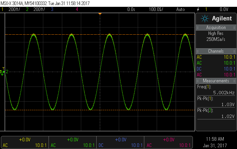
There are 4 files in the attachment. The customer uses 2 different amplitudes of the input signal with a fixed frequency=5KHz with the control input as HIGH and LOW Each. Yellow signal represents the input signal and Green signal represents the output signal. The details with respect to the filenames are as follows:

The first waveform: 1vppoff - This represents the i/p and o/p signal with 1vpp input amplitude and the control pin=OFF.

The second waveform: 1vppon - This represents the i/p and o/p signal with 1vpp input amplitude and the control pin=ON.

The third waveform: 2vppoff - This represents the i/p and o/p signal with 2vpp input amplitude and the control pin=OFF.

The fourth waveform :2vppon - This represents the i/p and o/p signal with 2vpp input amplitude and the control pin=ON.

Case1: If the input is high and the control is high, then output should be high.  Here if the input voltage is increase to 2Vpp and higher, we see that the lower part of the output signal got clipped.

Case2.: If the input is high and the control is low, then output should be low right(i.e no signal at the output whatever the input voltage is)? Here we see that when the input is high and the output is low, we see that instead of giving a low output (~0 V), the output shows some signal around 450mVpp for 2Vpp Input voltage.
Q1: Are the case1 and case2 normal for CD4066B?
Q2: If the case1 and case2 are unnormal, can you clarify about the case1 and case2? How to solve the two issues?

Best Wishes,
Mickey Zhang
Asia Customer Support Center
Texas Instruments

  • Hello Mickey,

    The behavior you are observing is not expected.  Can you provide a schematic or at least a simplified representation of what you have connected to the various pins of the CD4066B?

  • Hi Patrick,

    Please check the attachment. VDD is 5V or 12V. VSS is connected to GND.

  • Hello Mickey,

    The clipping you are seeing at the trough of your input signal can be attributed to the fact that you are operating outside of the recommended ranges.  You are operating within the absolute maximum values, however, these values in the datasheet only correspond to the range of values that will not lead to permanent damage of the device.   Within the range of these values is a smaller range of values under which the device will exhibit proper behavior.  This smaller range is typically listed under the recommended operating conditions.  Unfortunately through the years not all datasheets were made as intuitive or complete, in which case (such as with this datasheet), you will need to check the test conditions for various parameters in the electrical characteristics section.  As in Table 1, this device is characterized with the channel input between 0 and Vdd.  From your scope shots, we see that you are trying to pass a 1 V pk-pk signal that straddles zero. As the signal approaches -0.5V the internal diode clamps the voltage at ~ -0.5V.  If you translated your voltage up 0.5V, you most likely would not see this clipping.  Also, its possible that because you are operating outside of the recommended range, this range of operation may be contributing to the large leakage currents you are observing.

    Table 1

    If you do not want to level translate your signal or give it an offset, perhaps you may consider one of our switches that has a negative supply.  You might consider our CD54HC4316. It also has 4 switching channels.  However, its upper rail is limited to 6V, which means you will need to do some sort of power conditioning if you use the 12V supply.