This thread has been locked.

If you have a related question, please click the "Ask a related question" button in the top right corner. The newly created question will be automatically linked to this question.

SN74CB3Q3125: SN74CB3Q3125 Isolation Characteristic

Part Number: SN74CB3Q3125

Hi,

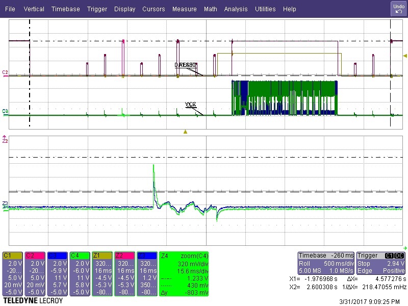
I am trying to understand why I see some a short voltage spike at the output of the SN74CB3Q3125 in the switch off state. 

Red Trace: Input to Switch

Gold Trace: Enable Signal

Green Trace: Output Signal from Switch (Zoomed in signal)

First voltage toggle is 1.8V, second voltage toggle is 3.3V, third voltage toggle is 5V. 

During the rise of the voltage toggle 5V, the switch output shows a ~1V spike. I was under the impression I would get better isolation when the switch is off...

Thanks in advance for feedback.

  • Hello Yohan,

    To properly answer your question, could you provide some description of your circuit? Is it on a perf board, PCB, or bread board? Could you post how you are connecting this device and how you are driving it?

    Thanks for the extra details.

    John Louie
  • Here is a simplified model of a passive switch. There is always a parasitic feedthrough capacitance between analog input and output. Therefore, when you quickly toggle the analog input, some glitch will be observed at the analog output no matter whether the switch is off or on. 

    The glitch peak level depends 1.how fast you toggle the analog input. 2. the RC loading at the analog output side. At the analog output, the glitch peak of a fast ramp analog input will be higher than that of a slow ramp analog input. As for RC loaing, higher loading resistance and lower loading capacitance, or big R, small C, will lead higher glitch peak.

  • Hi,
    Thank you for the feedback. Nevertheless the component I am using is FET bsed switch. I would expect the channel to be fully open when turned off.

    Yohan
  • Hi,

    Thank you for the response. Unfortunately I cannot post a schematic of my design. What I am able to tell you is that the SN74CB3Q3125 has four inputs. Each input is being driving by signals coming from a smartcard driver (5V based). The output of the switch is to a connector of a smart card chip. I am trying to prevent the smartcard chip from seeing the connection sampling performed by the driver as shown in the scope plot. Vcc is tied to 3.3V with a bypass capacitor 0.01uF. This switch is 5V input tolerant. I have pull ups to the EN signals connected to 3.3V as they are controlled by an MCU. The PCB is a two layer board built professionally. I populated the raw pcb myself.

    What I am not understanding is if the device is FET based and when High Impedance the FET channel should be open, therefore providing isolation. Why am I seeing voltage on the output when the switch is in the off state?

    Thanks

    Yohan
  • Hi Yohan, 

    By using an electrical switch, you will be always having finite isolation performance between analog input and output. Slowing the signal edge rate by adding additional capacitors will be recommended. Slightly slowing edge rate normally gives you three benefits. First, it will give you better EMC performance. Second, the ringing effect on the signal chain and ground line will be significantly reduced. Last but not least, cross talk or input/output isolation performance will be significantly improved. 

  • Hi,

    Thank you for your feedback. Apologies but my question is still not getting answers. The answers that are being provided are very generic. I have read all your documentation provided on the website, nevertheless I would like to know why this component does not provide better isolation especially with me understanding the semiconductor physics behind a FET. Having a 1V feed through for a 5V TTL signal to me is a lot.

    Thanks

  • Hi Yohan,

    Sorry for not having your question answered properly. As you know the FET, when switch is on, the signal forward path is from source to drain. When the switch is off, there is still a signal forward path which is from Cgs to Cgd. Another feed forward path is from Csb to Cdb. When switch is off, both capacitive signal forward paths only exist at high frequency.

    1V peak glitch being present at your system are because 1. the 5V TTL signal switching edge is too fast; 2. the loading impedence at the output side is too high. For example, if the TTL is driven from 0 to 5V within 5ns and the loading impedence is thousands of Ohms, it would not be suprised to see 5V peak glitch at the output.