This thread has been locked.
If you have a related question, please click the "Ask a related question" button in the top right corner. The newly created question will be automatically linked to this question.
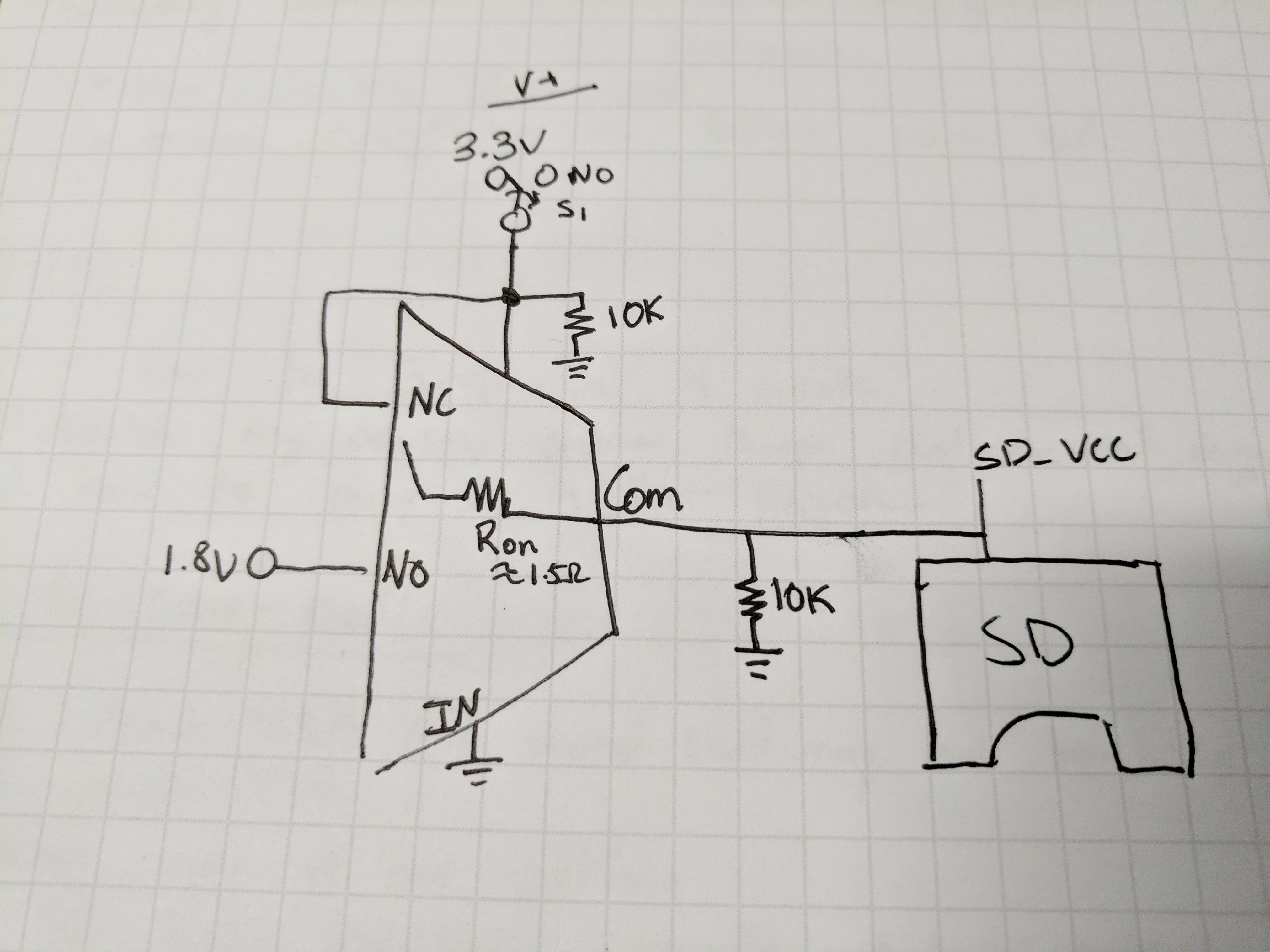
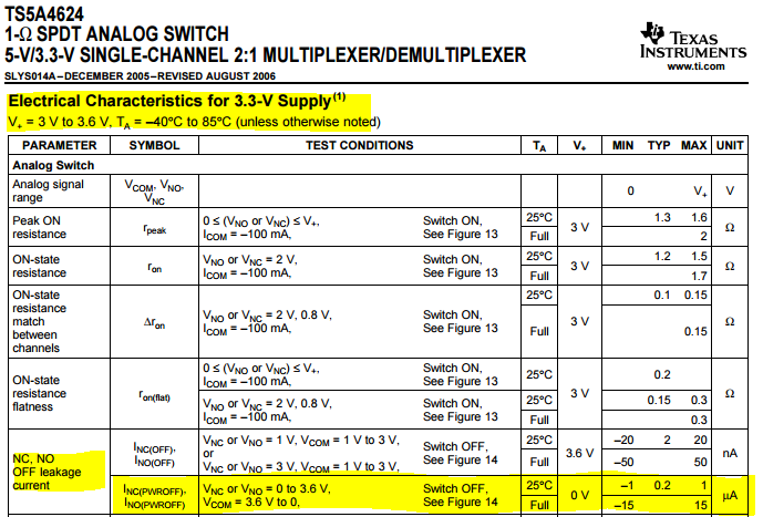
I'm trying to use this device as a low current power mux to deliver either 3.3V or 1.8V to an SD Card (details below).
However I have a condition when I would also like zero volts to be delivered to the SD card and would like to know how the device would behave under the particular conditions proposed below.
Could you please comment?
Now, if the proposed configuration wont work , could you please suggest an alternate configuration or different switch, also low cost, that could better meet this requirement?
Thank you,
Adam
Hi Dakotah
Thanks for your help.
Yes the intention is to select between 3.3v or 1.8v to power an SD card through the COM pin.
Load current is less than 100mA, so seems shouldnt be a problem based on the device ~1ohm rdson and 200mA current capability.
Now the question.
There is a use case where the 3.3V power to the SD card is removed (by a separate switch) and in this condition the switchable 3.3V/1.8V supply needs to be 0V. For the TS5A4624DCKR, there isn’t a separate enable input pin so I wanted to know how the switch will behave for the following condition:
V+ has weak pull-down resistor (10K ohms) to GND.
NC connected to V+.
NO = 1.8V.
IN = logic low.
COM has weak pull-down resistor (10K ohms) to GND.
What voltage will be present at COM?
Basically I am looking for low leakage current from 1.8V to COM when the device is not powered by 3.3V.
Hi Hector,
Thanks for clarifying your design intent.
You mentioned switching between 3.3V and 1.8V. You also mentioned having V+ tied to NC pin, from this I understand your V+ to be at 3.3V. I drew a quick diagram to ensure that I am understanding your system fully.
As you can see, I have 3.3V going through an external switch like you mentioned (your actual switch may a SPST) the 3.3V then goes through a weak pull down to GND, This is also connected to the NC pin. NO is tied to 1.8V. COM is connected to the SD_VCC and has a weak (10K) pull down to GND as well.
When 3.3V is removed from V+ the pull down resistor will pull V+ down to 0V. In this case you want to know the leakge current from the 1.8V input.
INC/NO PWR OFF is the power off protection spec. This spec states when VCC = 0V what the leakage current will be from the NC and NO pin. The table states this for a voltage at NC or NO up to 1.95V which would be the case for your 1.8V signal.
Here is a table for the power off proection leakage current if the voltage at the input pin is 3.3V (which I dont believe will happen in your system).
I also want to verify that you are using the 10K pull down on COM to pull SD_VCC to 0V when you are in this powered off state?
If any of that doesn't answer your question let me know and we can clarify anything.