This thread has been locked.

If you have a related question, please click the "Ask a related question" button in the top right corner. The newly created question will be automatically linked to this question.

Operating Outside of the Recommended Conditions With a negative signal

Part Number: SN74LV4051A

Hello,

Regarding to SN74LV4051, my customer is asking a question.


(Question)

When minus signal(0> Vio> -0.5V) is input, is output minus signal?

(For example: -0.2V -> Y0 pin-> COM pin -> -0.2V? )

On their application, it is possible that minus signal is input.

If this device is supported bidirectional, I guess that output will be minus signal at inputting minus signal.

Of course, we should consider Absolute Maximum Ratings (Vio> -0.5V).

Is this device is supported bidirectional?

And My understanding is correct?


Regards,

Tao2199

  • Hello Tao,

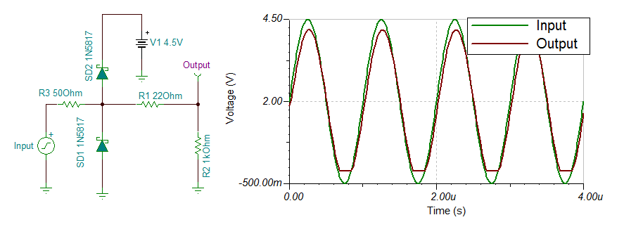
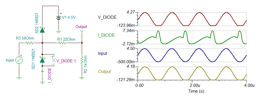
    The SN74LV4051A is bidirectional.  If the input is negative, the output should also be negative.  However, the output will not be identical to input.  Depending on your Vcc, source impedance, and load impedance, the output observed will be attenuated and possibly distorted.  The degree of attenuation observed will be determined by your Vcc.  Vcc sets the value of the Ron, the parasitic resistance of the switch, which forms a voltage divider with your load.  Distortion may be observed in the form of clipping which is a byproduct of the ESD protection diodes that are included in the switch.  Typically any device that defines that the input or output voltage can go 0.5V above Vcc or 0.5 below ground (table 1) will have these diodes or some other form of ESD protection.  The forward voltage of these diodes will determine at what voltage level your signal will be clipped.  An example of this can be observed in figures 1 and 2 below.  Our datasheets do not include much information on our protection diodes as they are intended as a protective measure for a device that may occasionally experience conditions where the signal is outside of the recommended operating range.  TI does not guarantee normal switch operation outside of the recommended operating conditions,  yet it could be observed depending on your loading conditions.  To determine if your signal would be passed sufficiently for your needs, the SN74LV4051A would need to be tested for your conditions: signal amplitude, bias, input impedance, output impedance, Vcc, expected temperature range.

    Table 1

    Figure 1


    Figure 2


    Figures 1 are not completely indicative of what will happen with the SN74LV4051A as this is not an exact replica of the devices internal structure.  In these figures, 22 ohm represents the typical Ron observed for the SN74LV4051A powered with a VCC of 4.5V,  50 ohm is the source impedance, and 1kohm is the load impedance.  The 1N5821 diodes are analogous to the ESD diodes found in the SN74LV4051A, however their specs are different.  You can see in this model, that once a certain coltage is reached, the diodes are forward biased and will clip the signal.