This thread has been locked.

If you have a related question, please click the "Ask a related question" button in the top right corner. The newly created question will be automatically linked to this question.

How to achieve the highest drive current at the output of the buffer

Other Parts Discussed in Thread: SN74LVC244A, SN74LVC1G125, SN74LVC827A, SN74LVC1G34, TPS3808

Hi..

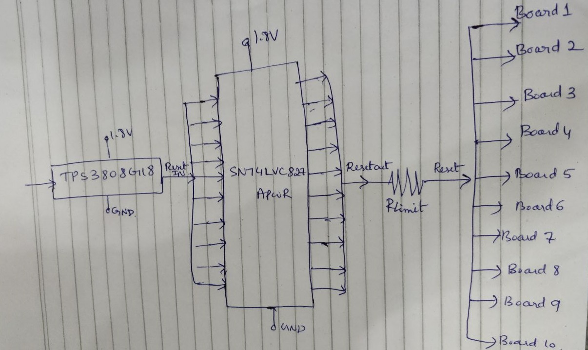
i am using SN74LVC827APWR with 10input & 10 output buffer, to drive reset signals to 10# high speed signal cards by using signal reset switch .

Requirement :

Reset signal voltage level is 1.8v (VCC)
Reset switch ouput is shorted to all 10 input of this buffer.
i planned to short all outputs of the buffer so that i can achieve the highest drive current at the output as well as required current to drive 10# different high speed signal cards.
if it is not possible in the above part (SN74LVC827APWR) please suggest me any other part where i can able to short all the inputs to single reset in signal and all the outputs to single reset out in order to achieve the required drive strength.

Thanks & regards,
Divya

  • Hello Divya,

    For our buffers, as long as the inputs are tied to the same signal, it is fine for the outputs to be connected in parallel. You should only do this for a single package, and you should not tie outputs of separate devices together as there may be slight differences in timing.

    Please note that the outputs are capable of driving more current than the channels themselves are rated for, so you have to have something on the output that limits the current.
    Furthermore, there is a maximum current through VCC or GND through the entire device of 100mA (in the absolute maximum ratings of the datasheet) so you cannot drive more than 100mA with this device total.

    If you need to drive up to 100mA then you could use the SN74LVC244A device:
    www.ti.com/.../SN74LVC244A

    How much current do you need to drive in your application?
    Maybe I can help to find a more suitable part if you need very high drive.

    Best,
    Michael
  • Please find the reset rough sketch in the attachment.
    As per buffer IC Datasheet i/p Cap is 5PF. hence we are shorting all i/p then the total cap becomes 50pF. These i/p are connected to the o/p of the supervisor IC (TPS3808G18DBVR), where o/p cap of the this IC not mentioned in Datasheet . can we interface or it cause any problem?
    buffer IC o/p Cap is 7P. hence we are shrting all o/p then the total cap becomes 70pF. these o/p are connected to 10# cards, where total i/p cap is 138pF. So O/P cap is less than that of the input cap. whether it causes any problem ?
    In Buffer IC datasheet we found the per pin drive strength as 4mA at 1.8V vcc supply.
    we need only 150uA . so this current is sufficient for us.
    What value of Limiting resistor will help us, so that it should not affect the o/p capacitance.

    Thanks & regards,

    Divya

  • Hi Michael,

    Please provide the solution for the above query.

    Thanks & regards,

    Divya

  • Hi Divya,
    Have you considered using a single SN74LVC1G34 (or SN74LVC1G125 if you need the OE pin) instead of the parallelled channels of the SN74LVC827A?

    The SN74LVC1G34 is rated for much higher output current and will drive heavier loads without adding all the extraneous parasitics of your current setup.
  • Hi,

    Thank u for your quick reply.

    I have gone through the SN74LVC1G125 &SN74LVC1G34 part datasheet. In datasheet pin output capacitance is not at all mentioned.

    From the datasheet we found test condition, which is provided only  for the load capacitance upto 50pF.

    As per our application we need to drive the 10 input pins,whose total input capacitance is more than 100pF. Is these part are able to drive this load capacitance ?

    If it is possible then tpd = ?

    Thanks & regards,

    Divya

  • The LVC family has very strong output drivers and is commonly used to drive 15+ CMOS inputs for fanout requirements (which is what you are describing).

    The output capacitance is typically 5pF for LVC devices.

    I would recommend testing with a prototype if you need specific timing data, but just looking at the datasheet values, it appears that there is a negligible change in the tpd of the device from a 15pF load to a 50pF load. If your system is sensitive to changes of < 10ns in this buffer, you might consider a redesign since we can't guarantee anything beyond the min/max values given on the datasheet (and they have a 6.3ns difference over process & temperature at 1.8V).
  • Hi Emrys Maier,

    Thanks for your quick response.

    we are ok with this buffer.

    we are using to drive the reset signal, so it may not be sensitive to our systems.

    One more clarification i want.

    Reset is generating from TPS3808G18DBVR. whether  it is possible to drive the reset signal directly from this device to 10 input devices without buffer  ?

    we are providing 100K pull up at the reset pin, because it is an open drain output.

    Please suggest wheher i can prceed with only TPS3808 without buffer OR With buffer.

    Thanks & regards,

    Divya

  • Hi Divya,
    Please post a new thread for your questions on the TPS3808 - that device is handled by our power management specialists.