This thread has been locked.

If you have a related question, please click the "Ask a related question" button in the top right corner. The newly created question will be automatically linked to this question.

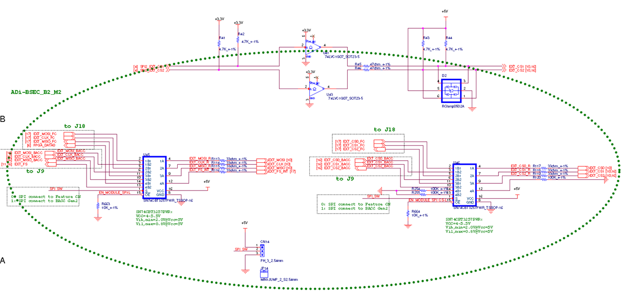
SN74CBT3257: 2-to-1 SPI switch design review

Part Number: SN74CBT3257

Hi Team,

I just want to double check for customer's schematics.

One of the SN74CBT3257 were using 3 channel for SPI de-multiplexer, 1 channel for GPIO multiplexer in the same chip, I think it's ok, correct me if wrong.

A bypass 0.1uF is suggested to add for both device Vcc pin, correct?

Anything else, feel free to add comment, thanks a lot!

Andrew

  • Andrew,

    All 4 signal paths are the same in the SN74CBT3257 so you may support multiple types of signals in a single IC. 

    I'm guessing the issue you may be concerned with is the clock signals crossing onto the GPIO?   The SN7CBTXXXX devices have ~-53dB of cross talk performance so you should no have much of an issue. 


    Something you should also be aware of is the SN74CBTXXXX devices are single FET switches and will not pass signals from 0V to Vcc but 0 to ~Vcc-1 V.  Usually this is not an issue because the transmitter and receiver Vih and Vil thresholds are not close to Vcc. 

    Looking at the schematic:

    Vcc = 5V which is within the recommended operating conditions.  It is standard practice to place a bypass capacitor as close to the Vcc pin as possible

    OE is pulled low by default which will enable all the signal paths

    S pin does not have a default pull up or pull down so there cannot be a guaranteed signal path that is selected during power up

    Please ensure the voltages on the signal path are within the recommended operating conditions and that your system does not require a Vih value of > 4V

    Thank you,

    Adam