This thread has been locked.

If you have a related question, please click the "Ask a related question" button in the top right corner. The newly created question will be automatically linked to this question.

TS5MP645: PCB tracing

Part Number: TS5MP645

Hi,

I'm designing a board that should have some form of switch between one MIPI source two receivers. TS5MP645 looks promising but I have some issues with routing PCB.

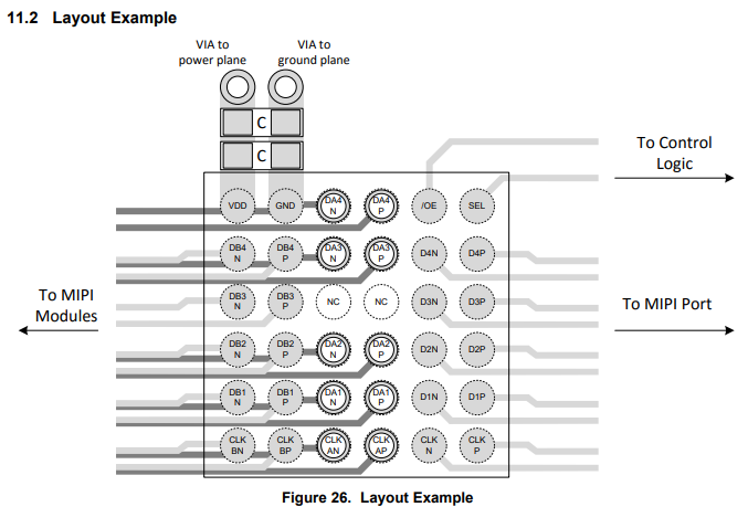
There are two examples shown - one presented in datasheet (page 22) is not manufacturable, and the second one used in evaluation kit has single lane differential signals on different layers.

I would appreciate advice how to make those connections properly.

Thanks in advance,

Jarek

  • Hi Jaroslaw,

    I'm glad the TSMP645  looks promising for your design. What is driving the need for multiple MIPI receivers in your system?

    Can you elaborate on why the pinout in the datasheet (page 22) is not manufactuable?

    The EVM online is for DC testing only.  Here is an application note on highspeed layout design.

  • Hello Dakotah,

    Thank you for a reply.
    I think I'm missing something basic. On Fig26 it looks like all signals of a given port are on the same layer. What should be parameters of track width and spacing to be able to route the signal like DB1P outside the chip?

    Best Regards
    Jarek
  • Hi Jarek,

    The parameters for trace width and spacing are typically limited by the manufacturing capabilities of your PCB manufacturer. The capabilities can vary widely and I would recommend finding out your tolerances and implementing those into your design rules.

    Based on your capabilities you can move to doing VIAs in the pad to fan out the BGA connections to other layers - this can make for a layout that isnt as dependent on trace width/spacing.

    Here is BGA routing app note for 0.4mm pitch for your reference - different implementations are discussed for proper BGA fanout.