This thread has been locked.

If you have a related question, please click the "Ask a related question" button in the top right corner. The newly created question will be automatically linked to this question.

CD74HC4051: Datasheet Inconsistency???

Part Number: CD74HC4051

Hello,

I am looking and studying your wide variety of analog mux/demux products. I need one for my Arduino project. I came across with the CD74HC4051 device ( found in http://www.ti.com/lit/ds/symlink/cd74hc4051.pdf ). 

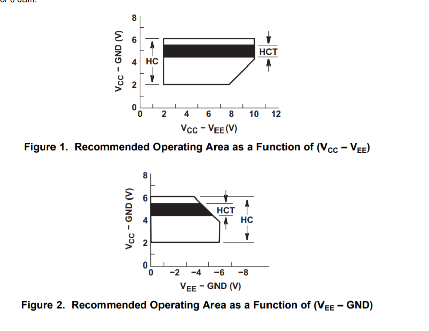
I just don't understand why the minimum value for VEE is equal to 0 V and the maximum value is -6.0 V? Shouldn't it be: min = - 6.0 V and and max = 0 V ? Likewise, given the values for VEE, [-6, 0], I don't think you can construct that graph shown in Figure1. That is, the only valid value for VCC is 2  at point where VCC - VEE equals 2. Simply put,  Figures 1 and 2 are contradicting each other. 

Please educate me on this matter. Thank you.

  • Abe,

    You can think of the recommended operating conditions table stating the max and min potential difference between the different supply pins.  You can't have more that a potential difference of 10V across this device but you can split up that 10V with dual supply rails that are asymmetric.  Also any one supply rail can't have more than a potential difference of 6 V to ground.   For example you can have 2 V on Vcc and -8V on Vee or 6 on Vcc and -4 on Vee.  Also you need at least a potential difference of 2 V across the device for it to operate.

    What are you needing to connect to your Arduino?  What is the voltage range, current, and signal bandwidth?

    Thank you,

    Adam 

  • Thank you Adam for your immediate response.

    I surely did get your point. However, I still don't agree on how the numbers were labeled and how the graphs were constructed ( if I am not mistaken with my Analytic Geometry and Calculus). Anyhow, I will further investigate on this matter.

    You mentioned that I can have dual supply rails that are asymmetric. Does that mean I can shift my GND to another level?

    For Example: (i) Set the VCC supply to +6.0 V and set VEE to -4.0 V.
    (ii) Force +1.0 V to GND pin.

    With that setup, I believe an asymmetric maximum analog signal of ten (10) volts peak-to-peak can be controlled. Is this methodology logical and would have the device operate and function properly?

    I would appreciate a reply on this. Thank you very much.
  • Abe,

    You may always shift your ground in any circuit but you will need to be extra careful not to violate anything by moving the reference.  For example with this specific IC, lets take the logic control spec Vih and Vil.  These values are specified with reference to ground and you would need to adjust your system accordingly.  For this reason we don't recommended shifting your circuit reference because it is hard to keep track of all the consequences.

    What signals are you attempting to pass through the switch?  What are you connecting on either side of the device?  Do you have a diagram or schematic with your voltage rails and signal swing labeled?

    Adam