This thread has been locked.

If you have a related question, please click the "Ask a related question" button in the top right corner. The newly created question will be automatically linked to this question.

SN74LVC1G3157: Using this part as resistor divider feedback

Part Number: SN74LVC1G3157

Hi,

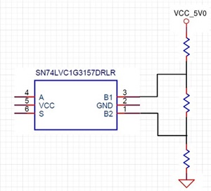
I am using this part as a resistor divider selector (see below).

The issue I am facing with is, when the supply of this IC is greater than 2.8V, the voltage that appears at Pin A when S = 0 and S = 1, is correct (based on resistor divider calculation).

However, when the supply of this IC drops below 2.8V, the voltage appearing at Pin A is not correct anymore.

Disconnecting either B1 or B2 from the resistor divider network will make the error goes away, and this leads me to think that below supply voltage of 2.8V, the resistance between B1 and B2 becomes

small enough to affect the overall resistance of the resistor in the center of the divider network. Is there any know issue using this part with B1 and B2 connecting to different part of the resistor divider network?

Any more suitable part to perform this function?

Thanks,

Alex.

  • Hi Alex,

    You are correct, the On resistance does increase when the supply voltage decreases. You can see this shown in the datasheet spec table for Ron across the signal range.

    When Supply voltage drops below 2.3V you can see the Ron increase up to 140Ω at 1.65V supply.

    How much this impacts your signal depends on the sizing of your resistors as well. Why is your supply voltage fluctuating so much?

  • Hi Dakotah,

    Thanks for your reply.

    I am not referring to the ON (channel) resistance, and the voltage I mentioned is 2.8V, which is greater than 2.3V.

    I am interested in the resistance between B1 and B2, not B1 (or B2) to A.

    The channel resistance will not affect my voltage divider reading because I am connecting Pin A to a high impedance load.

    Thanks,

    Alex.

  • HI Alex,

    Thanks for the additional details about the high impedance load. 

    There is no known issues with the input channels have an impact resistance as mentioned. 

    Can you please provide scope shots with the input and output signals to better allow us to understand the exact error you are facing?

  • Hi Dakotah,

    Thanks for your reply again.

    I have no scope data at the moment. I will try to capture some waveform.

    Some additional info that might help.

    All 3 resistors are 100K. Which means voltage at B2 is 1.67V, and voltage at B1 is 3.33V..

    The input S is tied to ground.

    I tested the circuit at 3.3V supply to the IC, the voltage at Pin A is correct at 1.67V..

    However, when I test the circuit at 2.8V supply, the voltage at Pin A is 1.8V.

    ( I did not check the voltage at B2. I will check it when I got the chance, but I believe it should also be at 1.8V).

    This leads me to think that there is a resistance between B1 and B2 that, when put in parallel with the middle resistor, cause the overall voltage divider resistance to be reduced, and therefore increasing the voltage at B2 (and also Pin A).

  • The recommended operating conditions do not allow the voltage at B1 to exceed VCC. (A current will flow from the pin through the ESD protection diode into VCC.)

  • My apology. I was trying to simplify my explanation. The resistors value are in such a way that the voltage appear at B1 and B2 will not be more than 2.0V.

    I was trying to say that the voltage appearing at A is not what the resistor divider value is set to. Thanks.

  • Hi Alex,

    Can you please provide the schematic drawing again with the actual resistor values included? As well as scope shots with the all the inputs and outputs being probed.