Because of the holidays, TI E2E™ design support forum responses will be delayed from Dec. 25 through Jan. 2. Thank you for your patience.

This thread has been locked.

If you have a related question, please click the "Ask a related question" button in the top right corner. The newly created question will be automatically linked to this question.

TS5A23166: TS5A23166 Absolute Max Ratings

Part Number: TS5A23166

I'm designing a bit of protection for an ADC to deal with inputs which may be powered when the part is not.  It appears by the verbiage that the TS5A23166 will get the job done.  Yet, as I was going over the data sheet, I became a bit confused by the absolute maximum ratings which state that, for the analog voltages (NO, COM) the maximum is V+ + 0.5V.  It amends this by stating that the rating can be exceeded if the clamp current maximums are respected.   As described in "Features", the maximum input voltage for the analog signals is not, in fact, limited by the supply voltage (but, likely, some other structure (zener?) which sets the voltage at which the clamp occurs).  For example ICs in TIs LVC logic family (which tolerate inputs when VCC is 0V) list their AMR as +6.5V (not related to VCC).

I hope this doesn't come across as picking nits.  As I read the spec, the AMR leaves me not knowing at what voltage an input would clamp.  Do I have do add current limiting on the driven side of the switch to ensure that the switch (and my analog source) are protected when unpowered?  

  • Hi Chris,

    Thanks for using e2e.

    If you look at the Note 4 and 5 in the Abs max rating for the TS5A23166, they are referring to the ESD protection diodes inside the device that channel excess current to GND (through reverse breakdown) or VCC (through forward biasing) when the input voltage approaches unsafe levels. The intent is to protect against damaging conditions in the internal circuitry.

    For the Analog voltage spec below,  an input higher than VCC or lower than -0.5V is not allowed unless there is a series resistor limiting the current into the input to less than the +/- IIK clamp current rating.

    The spec IIK in the table above describes the current limit out of the device (negative values) through ESD diodes

    Here is a good  link to show how to use the internal diode, or an external diode to clamp the voltage, or use a series resistor to limit the current.

    Regards

    Saminah

  • Thank you for responding, Seminah.  I will contend that if the internal ESD structures are as you describe. then the analog input would simply back-power the TS5A23166 (even with the small resistor (100ohm) used to limit the current through the ESD diode to 50mA).  I.e. V+ = Vno - 0.7V which, at higher voltages, would turn the part on.  Further, the leakage current spec, would also have to include the supply current of the part.  

    I'm afraid I'm even more confused now.  It sounds like any voltage on my analog input will back-power my low-power system; which is less than desirable.  


  • Hi Chris,

    It depends on the input signal for your application. Can you share what input voltage you are using for your application. I can then recommend a part with higher signal range.

    The values in the absolute maximum ratings table are simulated over process corners, voltage ranges, and temperature.  These abs max ratings are will not damage the device and are guaranteed by design.  However, the recommended operating conditions are the parameters that we guarantee the part will operate as characterized through out the datasheet.   

    Regards

    Saminah

  • Hello, Saminah.

    My supply voltage will be 3.3V and the analog signal range will be 0 - 3.3V.  However, the analog signal may be present when the supply voltage is not.  For this reason, I am looking for an analog mux or switch which is tolerant to input voltage when the V+/VCC is unpowered, without back-powering either the part nor the switch/mux output. 

    Were this a logic input, I'd simply grab a 74LVCxxxx part which only has low-side protection diodes thus allowing the input voltage to rise to 5.5V regardless of the state of the VCC pin.  I had assumed that is what  TS5A23166 did as well, given the description, but per the AMR and your description of the protection diodes, it sounds like I was wrong.

    Chris

  • Section 1 of the datasheet says "Isolation in Powered-Down Mode, V+ = 0", and the electrical characteristics INO(PWROFF) and ICOM(PWROFF) show that applying voltages to the analog pins in the power-off state is allowed.

    The datasheet contradicts itself. Saminah, can you please find out which specification is actually true?

  • Hi Clemens, Chris,

    Let me clarify the details:

    When there is no supply voltage, at 0V, the TS5A23166 offers powered-off protection and will maintain high-impedance state on the I/O pins and digital logic pins.

    The highlighted spec in the Electrical tables shows the leakage current when V+ is 0.

    Chris, since the input for your application is from 0-3V, you can use the TS5A23166 which will offer powered off protection when there is no supply (based on V+=0V spec in the datasheet).

    Regards

    Saminah

  • Saminah,

    I assure you, I have read through the specification, repeatedly, so continuing to reference it doesn't help to clarify my (our) understanding.  Here is my contention.

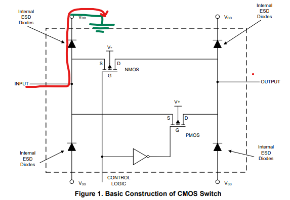
    1. If the part has high-side clamping diodes, as you contend, then, when the supply is unpowered, and the input voltage exceeds a diode drop (~0.7V) then current will flow through the diode to the Vdd pin (see Figure 1, below). In this case, there is no isolation to the input or output pins unless the input/output voltage is less than 0.7V. Is this clear? 
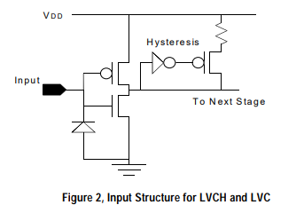
    2. The alternative is that this part has an LVC-style ESD clamping (see Figure 2, below) with only low-side diodes (possibly zeners) which mean there is no conduction path to Vdd, when the part is unpowered. In this case, isolation is possible over the supply range.

    If A is correct, then there is no isolation and the spec is wrong in suggesting that there is when the input and/or output greater than Vdd+~0.7. A series resistor will keep the current below limits and prevent latch up.  

    If B is correct, then isolation over the entire supply range is possible, BUT the absolute maximum rating is NOT dependent on Vdd and should be a fixed voltage (let’s say 6.5V for the sake of argument).

    Yet, both A and B cannot be correct as the spec is suggesting.

    Figure 1 – Standard ESD clamping diodes

    Figure 2 – LVC style with only low-side clamping

  • Hi Chris,

    Any device that has the Ioff feature will set the inputs and outputs to high impedance when Vcc is 0V and cannot be back powered. TS5A23166 has the Ioff ( IPWROFF) spec highlighted above with the leakage current.

    I think the Abs max table IIK spec may have been confusing in this case. Here is what you need to check:

    If there is only a (–) current spec in the Abs Max table, then there is only a diode to Gnd, and device cannot be back-powered. This means there is no conduction path to Vdd, when the part is unpowered. In this case, isolation is possible over the supply range.

    Here is a good post to understand more about back powering through ESD diodes.

    Please let me know if this clarifies your question.

    Regards,

    Saminah


  • Thanks, Saminah!  That does clear it up for me and I'll know what to look for going forward. 

    I'd still argue that the Abs Max for Vno and Vcom should be 6.5V and not "V+ + 0.5V" in that it tells me that operating in this region essentially voids the warranty (implicit or implied).  But, I'll let it lie.

    Chris