Parasitic inductance due to the length of PCB traces can cause overshoot and ringing during switching events. The output voltage may briefly exceed the expected output voltage value, due to overshoot, before slightly oscillating and settling to the steady state value. According to the equation, V = L * di/dt, a change in current over a short period of time, such as a switching event, will cause a voltage spike on the order of the parasitic inductance of the trace. This is the cause of the overshoot or ringing effects.
A large overshoot can have an impact on any system. Overshoot may cause damage to components downstream in the system, increase system settling time, or cause signal measurement errors. Certain applications may be sensitive to overshoot events. For example, ultrasonic systems such as ultrasonic flow meters may be impacted by overshoot due to low voltage signals. Additionally, overshoot events can impact remote radio unit applications.
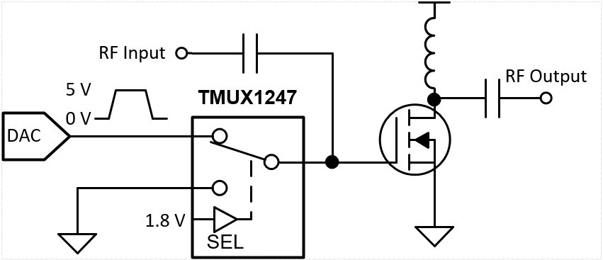
In remote radio unit applications, a switch can be used to control the input to a power amp stage for system level protection. Utilizing a device such as TMUX1247 allows a system to control when the DAC is connected to the power amplifier. The DAC output is utilized to bias the gate of the power amplifier with a 5V signal. The select pin of the switch can stop biasing the power amplifier by switching the gate to GND (0 V). The diagram below shows the TMUX1247 configured for control of the power amplifier.
Figure 1. Application diagram for input control of a power amplifier.
In cases with large parasitic inductances, the output of the switch may experience overshoot when switching from GND (0 V) to the DAC output voltage (5 V). There are several solutions that can be implemented to decrease or remove overshoot or ringing effects.
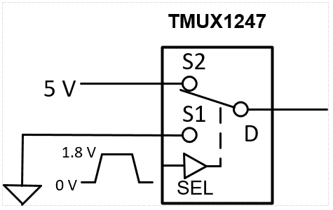
To replicate and measure the overshoot in TMUX1247, the test setup in Figure 2 was implemented. The supply voltage of the switch was 5 V. The output at the drain pin (D) was measured in the cases of switching from S1 (GND) to S2 (5 V) and switching from S2 to S1 using the select pin. The select high value was 1.8V and the select low value was 0V.
Figure 2. Test setup for measuring overshoot.
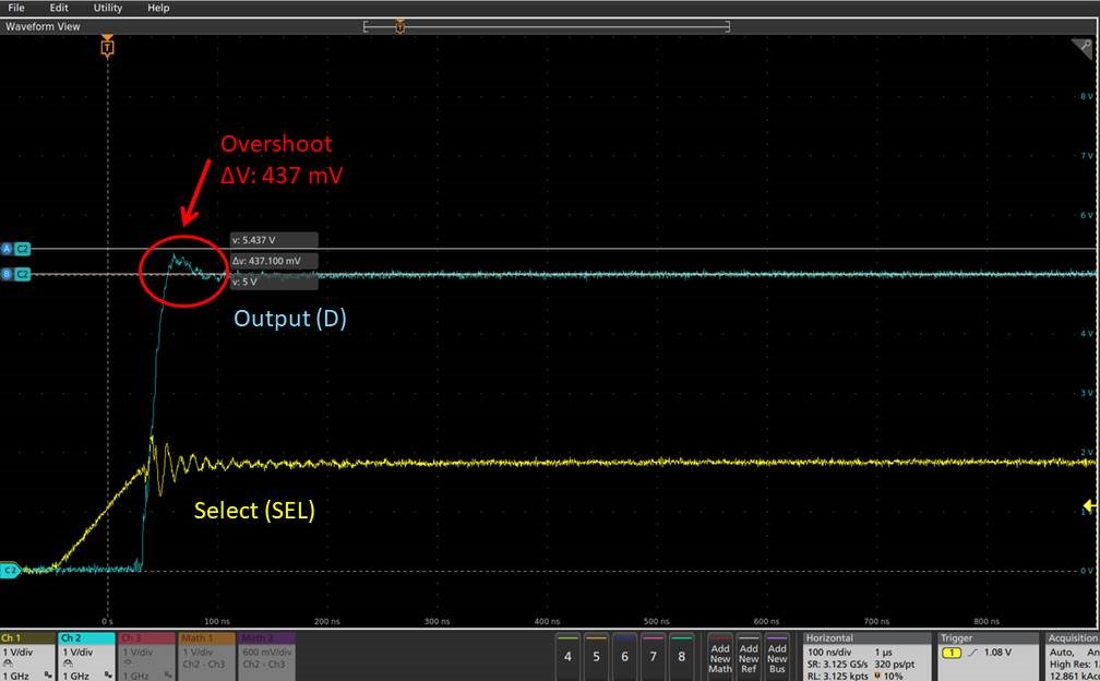
The scope shot in Figure 3 shows the switching response of TMUX1247. The select signal, the waveform in yellow, rises from low to high, causing the switch to switch from S1 to S2. The blue waveform is the output response of the switch. Note there is a positive overshoot of 437 mV, which could possibly cause damage to the system.
Figure 3. TMUX1247: Overshoot of rising output signal at drain pin.
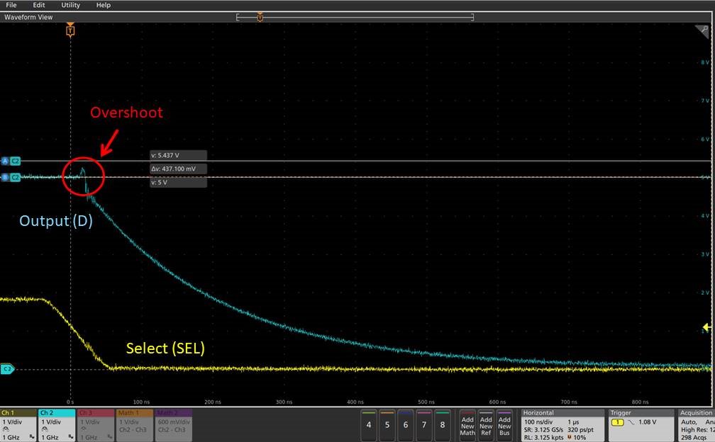
In addition, overshoot can be observed when toggling the select pin from high to low. The scope shot in Figure 4 shows the switching response of TMUX1247 as the select pin toggles from 1.8V to 0V. Note that overshoot also occurs on the falling edge of the output.
Figure 4. TMUX1247: Overshoot of falling output signal at drain pin.
Solution 1
It is important to consider several guidelines when designing the layout of your PCB to minimize overshoot and ringing. Implementing the following changes below will combat the common causes of overshoot due to trace parasitics.
- Decouple the VDD pin with a 0.1-µF capacitor, placed as close to the pin as possible. Make sure that the capacitor voltage rating is sufficient for the VDD supply.
- Keep the input lines as short as possible to reduce parasitic inductance and capacitance.
- Use a solid ground plane to help reduce electromagnetic interference (EMI) noise pickup.
- Do not run sensitive analog traces in parallel with digital traces. Avoid crossing digital and analog traces if possible, and only make perpendicular crossings when necessary.
- To reduce reflections due to traces turning corners, the best practice is to round the edge to keep the width of the trace consistent.
- Match load impedances with source impedances to minimize signal reflections.
Solution 2
Place a capacitor to ground at the drain pin of the switch. The capacitor value will vary with the amount of overshoot, but may be on the order of 100pF to 10nF. Additional capacitance will lower the effect of overshoot, but also impacts timing and settling requirements of the system.
Solution 3
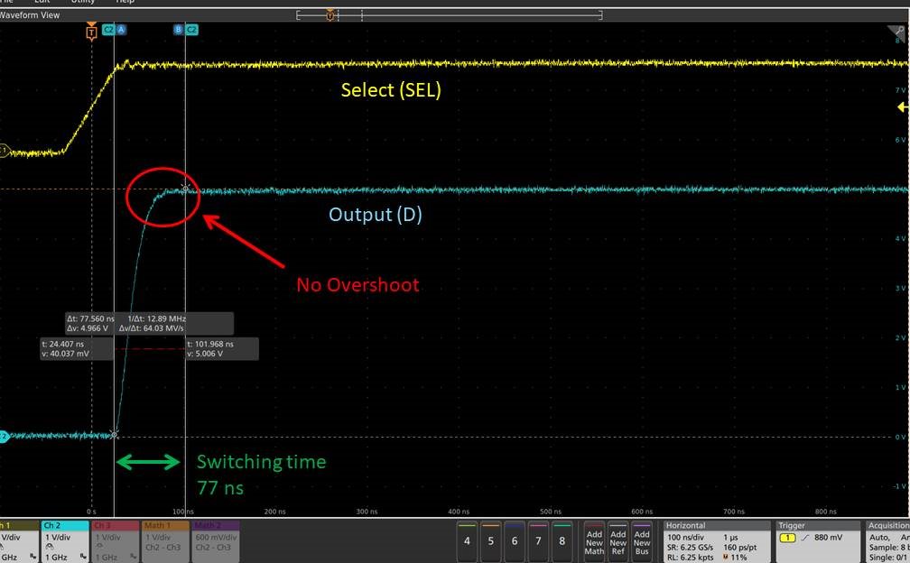
Another solution to prevent overshoot is to use TMUX1237, a new pin compatible device with TMUX1247 that is designed to prevent overshoot events. TMUX1237 is available for preview on TI.com now.
By replacing TMUX1247 with TMUX1237 in this test setup with the same supply and signal voltages, there was no overshoot observed at the drain pin when raising the select pin from low to high. The switching time was 77 ns, which is faster than the previously suggested solution of adding capacitance at the drain pin.
Figure 5. TMUX1237: No overshoot of rising output signal at drain pin.
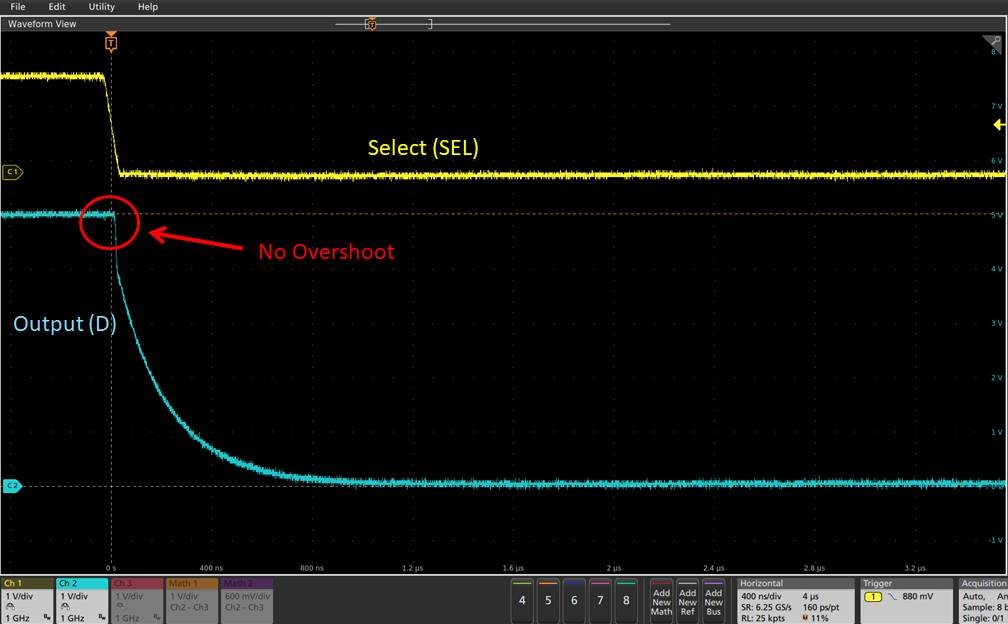
Additionally, there is no overshoot observed at the output of TMUX1237 when the select pin is toggled from high to low.
Figure 6. TMUX1237: No overshoot of falling output signal at drain pin.
If your system is sensitive to overshoot events, you may want to add a capacitor to the drain pin of the switch or redesign your PCB to align with the above suggestions. Or, if the configuration of TMUX1237 is compatible with your system, consider replacing your current device with the new TMUX1237.
TMUX1237 datasheet is available here.
Please see attached details on the qualification details.


