This thread has been locked.

If you have a related question, please click the "Ask a related question" button in the top right corner. The newly created question will be automatically linked to this question.

TMUX1104: Source/Drain Input Structure

Part Number: TMUX1104
Other Parts Discussed in Thread: TS3A5017, OPA2197

Hi,

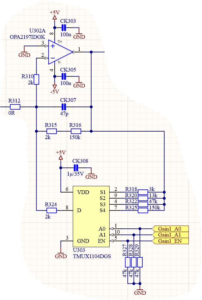
since the absolute maximum ratings for "Source or drain voltage (Sx, D)" are in the range of -0.5V to VDD+0.5V according to the TMUX1104 datasheet, I suppose there are some kind of ESD clamping diodes present at the source and drain inputs. Is that correct?

We are planning to use the TMUX1104 in an upcoming design and the problem is, that the part might be exposed to negative voltages at the source and drain pins under certain circumstances (error case). Are voltages beyond the absolute maximum ratings at the source/drain pins permissible as long as the input current ratings are observed (e.g. by limiting the input currents to <10mA by means of series resistors)?

Thanks and best regards,

Sebastian

  • Hi Sebastian,

    You are correct in your assumption that TMUX1104 includes ESD protection diodes. Take a look at this article about how to identify the internal diode structure by recognizing datasheet specifications.

    You have your new logic circuit running and everything works as designed. Then you turn off the power and the circuit continues to work. What is going on? In today’s world, with all the plug-and-play…
    By in Technical articles > Analog

    Take a look at this app note, System-Level Protection for High-Voltage Multiplexers, specifically section 2. This section describes what occurs internally during an overvoltage event and mentions that the I/O current should be limited to the abs max rating:

    To ensure device and system protection, ensure that the continuous current at the source and drain pins is within the +/-30mA absolute maximum rating, as shown below.

    What is your application for which you anticipate an error case of negative voltage at source and drain? How much negative voltage are you expecting at the source or drain pins?

    Best regards,
    Kate

  • Hi Kate,

    thank you very much for the quick response. The app-note is very helpful - good to know that the multiplexer input structures are no "black magic" :-). The ideas for clamping current limiting are very similar to those used with op-amps, actually.

    Concerning our target application, I cannot go too much into detail but the basic idea is to use the TMUX1104 for variable gain setting in a trans-impedance amplifier circuit (see part of the circuit below). Thing is, the multiplexer must exhibit very low-leakage currents and must operate from a 5V supply. Therefore, the TMUX1104 seems to be a very suitable choice at an acceptable price. This is also the reason why TS3A5017 (like suggested in your email) is not suitable in this case.

    Under normal conditions the current flow trough R312 will be from right to left, which will result in a positive voltage swing between 0V and 5V at the output (pin 1) of OPA2197, thus the source and drain pins of TMUX1104 will only see positive voltages too. Now, there is a small chance of inverse current flow through R312 (e.g. caused by false wiring), which would result in a negative voltage (-5V worst case) at OPA2197's output and the TMUX1104 source pins. In this (error) case the injected current trough the ESD-diode to GND would be limited by the series resistors at the source pins to below 2mA. From what I've learned from the app-note, this value is well below 20% of the TMUX1104's absolute maximum rating and therefore uncritical, even if the part is exposed to the error condition continuously.

    Just one more question concerning a statement you wrote in the email, which got me a little confused in the end:

    quote: "However, because the datasheet does NOT specify I/O clamp current, there is no "exception" to absolute maximum ratings."

    The "Source or drain continuous current (Sx, D)" (±30mA for TMUX1104) rating also applies to clamping conditions where current is conducted through the internal ESD diodes. Is that correct?

    Thanks and best regards,

    Sebastian

  • Hi Sebastian,

    Thanks for that information! Your last statement is correct. The source and drain continuous current specification also applies to the clamping condition. 

    I actually updated my response to reflect this, as I had realized this after my initial post.

    Best regards,
    Kate