This thread has been locked.

If you have a related question, please click the "Ask a related question" button in the top right corner. The newly created question will be automatically linked to this question.

SN74LVC1G3157: Break Before Make Switchover

Part Number: SN74LVC1G3157
Other Parts Discussed in Thread: TMUX1237, , SN74LVC1G04

The SN74LVC1G3175 device datasheet lists the break-before-make feature.

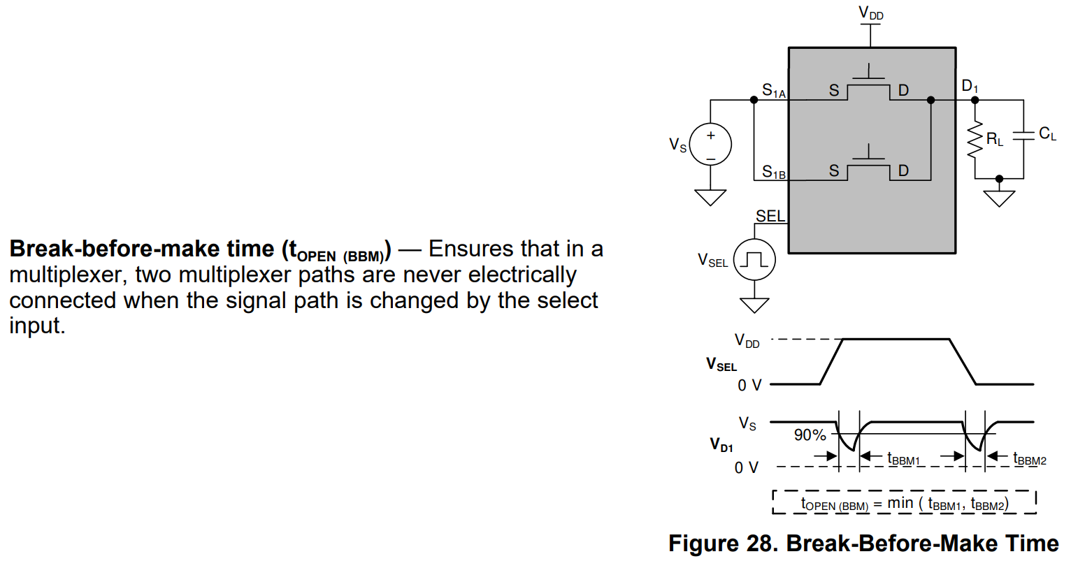
From literature found regarding the BBM feature, it seems power is removed from the output for a short time, when switching between channels, to prevent shorting channels together.

Because of this, the output voltage decays based on the time to discharge the output capacitance.

I am using this literature for reference: SLVAE51–November 2018

My questions is this:

1. With BBM, the output isn't shorted to GND or anything, right? Power is just disconnected, so whatever voltage the output was at, will decay as the charge stored in the output capacitance discharges through various paths to GND.


2. The SN74LVC1G3175 datasheet lists tB-M as MIN 0.5ns. What is this parameter exactly...? Figure 11 from the DS shows a parameter "td"...Is there a maximum switchover time parameter over temperature listed? This is needed to calculate how long the output capacitance will be discharging.

3. If you are switching between two similar voltages (say Ch-1 at 5V to Ch-2 at 5V), and want to minimize the voltage drop at the output, you would increase the output capacitance, right? 

4. From the literature SLVAE51, page 10, there are some equations and a graph depicting the expected Vout dip during the switchover process. Is my understanding below accurate?

For SN74LVC1G3175, the switchover time is XXX. I will assume 1ns MAX for now.
We will assume Iout when the output is 5V to be 1mA.
We will assume 30pF of output capacitance.

Then from the equations, Vdip = 1ns * (1mA / 30pF) = 0.03V

Thus, the output voltage will only dip 0.03V. Is this understanding accurate for break-before-make operation w/ such analog switches?

Regards,

Darren

  • Hi Darren,

    Thanks for your question regarding the BBM feature of this switch. I will take a look and post a response for you on Monday, September 28th.

    Best regards,
    Kate

  • Hi Darren,

    Thanks for your patience. I'm happy to address your thorough interest in the BBM feature.

    1. This is true; during a switching event, the output voltage will decay according to the output capacitance.
    2. The switching characteristic tB-M specifies the minimum internal timing that the switch output will be disconnected (labeled tD in Figure 11 of the datasheet). The BBM feature ensures that the switch's output will be disconnected for at least the minimum tB-M. You can use this minimum specification in your calculations. Also, you can learn more about switch timing characteristics, such as BBM delay, in this TI Precision Labs Video.
    1. Yes, this is a good idea.
    2. Your understanding of these equations is correct and the calculation may be used to estimate the voltage drop.

    What is your design application where you are concerned about BBM? I recommend taking a look at our new TMUX switches with break-before-make, such as TMUX1237, which is designed to prevent overshoot during switching events.

    Best regards,
    Kate

  • Hi Kate,

    I am still a little confused. It seems the tB-M max spec is needed to understand how long the channels are disconnected, and thus how long the output capacitor will be discharging. This will define the lowest output voltage dip seen.

    Do you have any characterization data for the MAX tB-M spec? Or at the very least, what is the longest tB-M time seen...?

  • Hi Darren,

    Thanks for the follow-up. I've included the break-before-make time definition from the Multiplexers and Signal Switches Glossary:

    Break-before-make time is always defined as the minimum time that the switch is "disconnected". As you can see from the timing diagram, tBBM is the time taken from the point when the output drops to 90% of its original value to the point that it rises to 90% of its expected value. tBBM is characterized for the set of load conditions in each device's datasheet, in the case of SN74LVC1G3157: RL = 50ohm, CL = 35 pF. The time taken to rise/fall also depends on these conditions.

    The BBM feature only ensures that there is indeed a minimum amount of time that the switch is "disconnected", therefore the exact amount of time [and voltage drop at the output] is dependent on your system and load conditions.

    Best regards,
    Kate

  • Hi Kate,

    That is helpful. Quick follow-up and I think I'm satisfied.

    From the above, tBBM is the minimum time between 90% falling, and 90% rising. This means the switch is actually "disconnected" for about 1/2 the tBBM time, right? (the switch is only disconnected for the time when the output voltage is falling; when the output voltage is rising, that means the switch has connected to the other channel)

    Would it be safe to assume that the actual switch disconnection time, is about 1/2 the tBBM time?

    And worst case, the actual disconnection time should not be more than tBBM?

    Darren

  • Hi Darren,

    Good question, however the "disconnection" time cannot be assumed/guaranteed to be 1/2 due to the differences in charging/discharging patterns of the external circuit. Because the BBM feature ensures the device will not short input signals, tBBM is included in the datasheet to indicate the minimum delay to be expected in the output voltage response at the specified conditions. As you pointed out before, the load capacitance and external circuit may be designed to minimalize the "drop" in voltage during switching and timing may shift accordingly.

    Best regards,
    Kate

  • Hi Kate, 

    Makes sense...assumptions are usually always a bad way to go...:)

    That said, could you help me understand one more point? How does the BBM feature actually work?
    I have been assuming there is internal circuitry that disconnects the channels for a certain amount of set time programmed by internal circuit structure, and that this time is relatively constant and independent of the output CL/RL. Whereas tBBM takes into consideration the output current draw and capacitance to charge before the output voltage reaches 0.9 x Vo again. This is dependent upon the output conditions, but the actual switch disconnect time is not - correct?

    It seems to me that knowing the MAX disconnect time (not the 90% to 90% fall/rise time given some load, but the actual switch disconnect time) is essential for calculating the output voltage dip, and making sure this value does not fall below the hysterisis voltage threshold level of the device the output is connected to.

    Because, as you mention above, CL and RL can be sized to minimize this drop, but honestly, without any ballpark range of the maximum switch disconnect time, you can't select the right CL and RL values...MAX could be 1ns, or it could be 100us. It could even be 2s! (I know it is not, but without this characterization data, there is no way to know) How do you select the values to limit the voltage drop, when you don't know how long the channels could be disconnected for...?

    Do you have any ballpark figure on the actual switch disconnect time, or can you confirm with the design team on this? I am not interested in the tBBM parameter, as this is dependent on the output CL/RL. I need to know the actual switch disconnect time (even a ballpark statement that "it should not be more than xxxns" is fine), please.

    Thanks,

    Darren

  • If you use an AND or OR gate where one input is connected directly to the input signal, and the other input is connected to the input signal through an even number of NOT gates, then the output will be the same as the input, but rising or falling edges are slightly delayed, due to the propagation delay of the inverters.

    So the maximum tBBM is the maximum propagation delay. You could look at the datasheet of the SN74LVC1G04 to find out what the spread might be. The gates of the MOSFETs in the switch are a smaller load than that datasheet's test condition, so the actual tBBM will be smaller.

  • Hi Kate, 

    Is it okay to go with Clemens statement that the tBBM MAX time will be less than the device propagation delay time?

    Regards, 

    Darren

  • Thanks for your input, Clemens.

    Darren, t(en) and t(dis) are the switching characteristics defined by the amount of time delay for the output to respond to a change in control input. You may use these max characteristics as a guideline for your design calculations.

    Best regards,
    Kate