


e2e,
I'd like to design MIPI CSI 4-lane D-PHY 2:1 MUX function by using TS5MP646 solution.
But we have a trouble to route PCB pattern from inner side 0.4pitch ball pad in TS5MP646.
There is no option to route DA#1/2/3 P/N lanes having adjacent reference layer for return path in our stack-up.
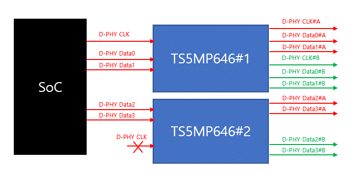
So, I'm thinking to use two TS5MP646 chips with splitting input data lanes like below picture.
Is this configuration is feasible? 2nd TS5MP646 chip won't have clock input, I'm not sure if it makes some problem or not.
Thank you,
Adam
