Hi,
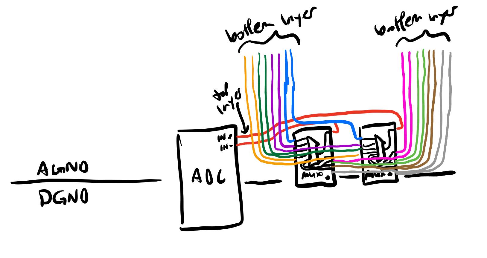
I am looking to use the TMUX1108 in a design with an ADC. I am currently planning on having a partitioned ground (AGND and DGND split, and connected at the ADC, analog power supply, etc), and am not clear on the proper layout of the TMUX1108 with regards to this. I would assume that the mux should also be placed across this partition, in line with the ADC and other ICs that have both digital and analog return currents (I have sketched what this would look like). However, as shown in my sketch, it would require these analog signals to border along the AGND and DGND partition. The slots in the PCB would also mean that a significant portion of the return current would not stay in the analog partition, and rather go through the digital partition, where it is susceptible to picking up noise and EMI. The alternative that I see is moving the mux to be completely within the analog partition, but this would result in digital signals in the analog partition. This may not be so bad as the address lines will likely remain relatively constant for the duration of the ADC conversion.
Is there a recommended layout between these two options, or a better way to do this? Thanks!