This thread has been locked.

If you have a related question, please click the "Ask a related question" button in the top right corner. The newly created question will be automatically linked to this question.

TMUX136: The bandwidth problem of analog switch chip tmux136

Part Number: TMUX136

1. What is the difference in bandwidth between a single tmux136 chip and three tmux136 chips in series, or the bandwidth is not affected by the multi-cascade of chips.

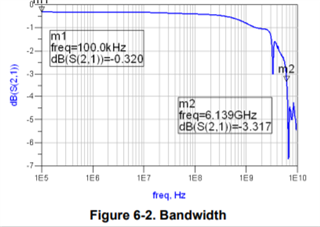
2. The bandwidth (-3dB) written in the specification: 6.1GHz. The Bandwidth graph also shows that when the bandwidth is within 1G, it is dB(S(2,1))>-0.5. The frequency response within 1G is very good. The above is a straight line, but we found that it is not. At 100MHz, there is a situation of dB(S(2,1))<-1.5. Does -3dB also appear periodically in the 1GHz bandwidth range.

3. If it can be achieved, what should be paid attention to when designing a multi-cascade chip, so that the bandwidth can reach the bandwidth shown in the Bandwidth curve of the specification. When the bandwidth shown in the Bandwidth curve of the specification is within 1G, it is dB(S(2,1))>-0.5, within 1G The frequency response is an approximate straight line.

4. Do you use the usual test method for testing bandwidth, and if not, what test method do you use?

  • Hi Dongdong,

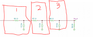
    1. The switches are passive and low impedance - cascading multiple in series is going to degrade the bandwidth. Loading conditions of the multiplexer also affect bandwidth. Please see below for a simplified circuit model of 3 TMUX136 in series:

    Each mux is represented by the worst case On resistance in the datasheet and worst case capacitance (13 Ohms (port B max resistance) and 2pF (worst case on capacitance). At worst case conditions this simulated (with a 50 ohm load) at about a -3dB of 1.92GHz - showing a large reduction by cascading the multiplexers. 

    If you aren't running at max conditions the bandwidth will improve - but it will still be a degraded BW with respect to the typical number found in the datasheet.

    However layout and other sources of capacitance (layout, loading conditions of the multiplexer) will degrade the signal further as more capacitance on the bus will reduce the BW. 

    The BW numbers represented also remove Insertion loss from the equation as there will be DC level loss. So the -3dB is the point where the system is outputting a signal that has -3dB gain from the DC gain.

    2. We don't have a BW graph with 3 TMUX136's in series - but we do have a BW graph that is in the datasheet that shows the waveform:

    The bumps that you are seeing could be a due to cascading the devices in series and/or layout adding capacitance. The package itself also contains inductance which is increased by cascading parts which could cause a deviation from the above graph.

    3. It will be pretty hard to get the full bandwidth or close too full bandwidth when cascading parts as you are trying to do:

    i) Layout of system - the mux signal pathway should be as short as possible with impedance matched trace lengths (as it is a high speed design), capacitance is a large issue that must be mitigated during layout. 

    ii) Besides layout - creating high impedance stages in-between each multiplexer will improve bandwidth as the TMUX136 will have its highest bandwidth when the load is low capacitance and high impedance. Devices such as buffers can work in these applications to work. The only concern is to make sure that the buffers are rated at the same bandwidth as the mux as well as the same voltage range required. 

    If you implement high impedance stages in-between each mux to mux connection and keep the layout simple and low capacitance there is a lot better chance that you will achieve close to the 6.1GHz .

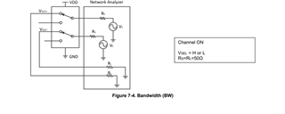
    4. Testing for bandwidth is as shown below (also included in the datasheet):

    with the following test conditions:

    If you have any other questions please let me know!

    Best,

    Parker Dodson

  • hi Parker,

        I am very happy to receive your reply, and I have a few more questions to ask.
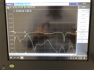
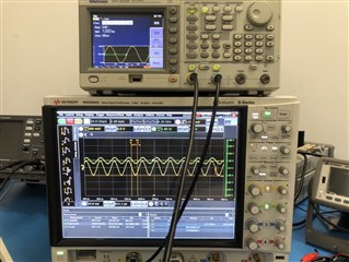
        Our measured bandwidth and amplitude are not very ideal. The parameters of S21 and S11 are very poor, reaching -3dB at 550MHz. The measured amplitude is reduced by half at 100MHz. This parameter is very different from the specification. what is the reason? Even if it is very bad, the actual measurement is not so bad. The test picture is as follows:

    with the following test conditions:

    VCC=3.3V,R=50Ω,Switch on

  • Hi Dongdong,

    Have you removed insertion loss from bandwidth plots?

    The typical resistance of the switch is 5.7 Ohms - At DC levels Vout = Vin * (50/(50 + 5.7 * 3)) ~ 0.7452 * Vin. This loss is removed from the bandwidth plot.  

    This will increase the bandwidth as we report it in our datasheets. 

    Package parasitics as well as layout parasitics also affect the BW. How are the TMUX136's laid out for the testing your are completing? Extra capacitance and inductance will also degrade bandwidth. 

    Is there a board that you have built that you are testing this on? Especially for high frequency design the layout can negatively impact BW - are all traces impedance matched? Is the source matched to the load? At higher speeds there are many external factors that can impact bandwidth.

    If you can show me the layout or how testing is being done I can see if there is other issues that may be able to be resolved with a change of layout. Also if you can confirm bandwidth after accounting for insertion loss it will give a clearer picture of where the part is actually operating at. However I still suggest buffers at each of the multiplexers output to increase bandwidth as this will mitigate insertion loss as the load to teh mux is Hi-Z. It also separates parasitic capacitances - preventing them from adding to one another decreasing the bandwidth by increasing the capacitive loading on the bus. 

    Best,

    Parker Dodson

  • hi Parker,

         I am very happy to receive your reply.

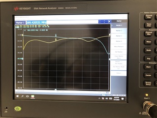
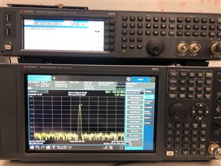
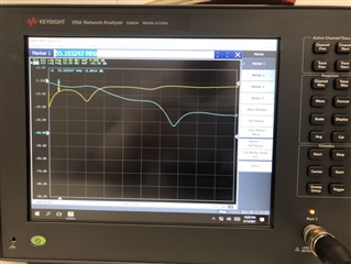
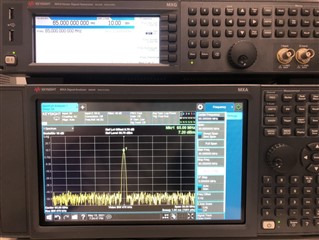
         During the test, the insertion loss has been eliminated from the bandwidth graph. Based on TMUX136, we designed a test board for testing. The test board uses TMUX136 chip three-cascade connection, and a total of 32 links are designed. Considering the use of RF signal generator as the source, It will be inaccurate to test with an oscilloscope. I changed the test method, used a network analyzer and a spectrum analyzer to test, used a network analyzer to test S11 and S21 to understand the bandwidth (-3dB), and then used an RF signal generator and a spectrum analyzer The measured bandwidth (-3dB), the two test results are basically the same. From the test results, the bandwidth of the three-cascade connection is very poor, which is far below the bandwidth required by us. The test pictures of two of them are as follows:

    1.A single TMUX136 chip in the entire link, no other components, but 16 branches in the link are reserved and not used:

    2.Three TMUX136 chips in the full link are cascaded. In addition, there are two 16 branches in the link that are reserved and not used. The reserved branches are necessary for our use and cannot be removed:

         Finally, based on our test results, it is judged that a three-cascade connection is used as a link. A total of 256 links are designed on a board. It is basically impossible to achieve a bandwidth of 1GHz for each link.

         So, I would like to ask you to confirm that the design scheme uses three cascades as a link, and a total of at least 128 links are designed on a board. Can each link reach a bandwidth of 1GHz? If it can be realized,give us a design layout and wiring reference.If it can't be achieved in actual use, please tell us directly and look for new solutions.

          Looking forward to your reply, good luck!

  • Hi Dongdong,

    Theoretically you can cascade three of TMUX136 pathways in series and it can achieve a BW of at least 1GHz and realistically more - however in practice there are many nuances in the design that are required to achieve that bandwidth without using buffers in-between each stage of the mux. At 1GHz the layout becomes a huge issue especially with a high amount of IC's. Because of this and the fact that is isn't a super common use case of this multiplexer  we don't have any schematics or layouts to show and with the time required to design high frequency applications especially on the layout side we can't spare the resources to create the layout / design files requested.

    That being said there are a couple options you can pursue:

    -Re-examining the layout for possible changes. Using High Speed Analysis software tools would be very helpful to understand how the signal is moving through the conductor. I have attached two high speed layout guidelines that while not specifically about multiplexers - have a lot of good general advice.

    scaa082a-highSpeedLayout.pdfspraar7h-highSpeedInterface_layout.pdf

    Also - another option is to add high speed buffers in-between each mux stage this will help prevent loading affects of each multiplexer on one another.

    If you have any other questions please let me know.

    Best,

    Parker Dodson