This thread has been locked.

If you have a related question, please click the "Ask a related question" button in the top right corner. The newly created question will be automatically linked to this question.

Cross-triggering between ARM and DSP

Other Parts Discussed in Thread: 66AK2H12, AM5728, 66AK2H14

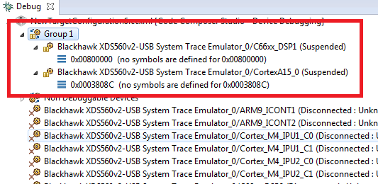
I'm wondering if arm_A15 and C66xx can pass debug events to each other.

For example, is it possible that breakpoint event in ARM stops DSP and vice versa?

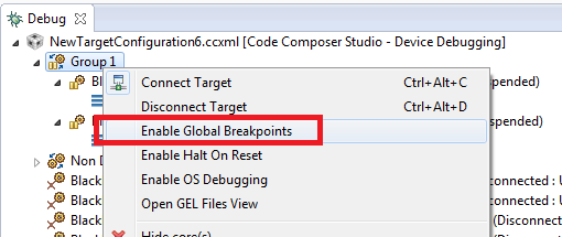
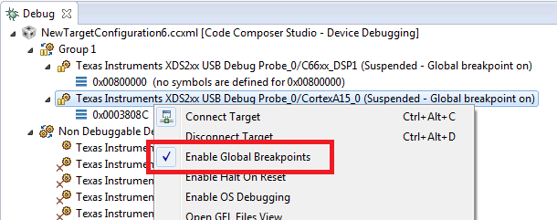
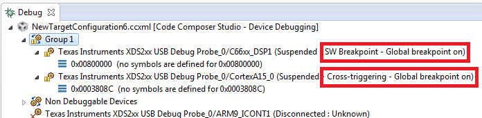
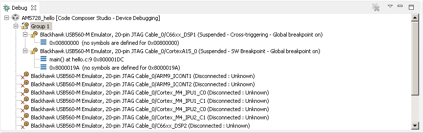
If possible, please let me know how to setup CCS to enable cross-triggering between ARM and DSP.

My development environment:

  Host OS: Windows 7 64-bit

  CCS Version: 6.1.3.00034

  Board: EVMK2H

Regards,

Park.

  • Hello,

    HS Park said:
    For example, is it possible that breakpoint event in ARM stops DSP and vice versa?

    Yes, this is also known as global breakpoints and should be supported between both homogeneous and heterogeneous processors on the same JTAG scan chain.

    http://processors.wiki.ti.com/index.php/Multi-Core_Debug_with_CCS#Global_Breakpoints

    Thanks

    ki

  • Thanks for your reply.

    But I cannot enable global breakpoints for ARM and DSP simultaneously.

    I just can enable global breakpoints only for ARM CPUs or DSP CPUs.

    If I select "Enable Global Breakpoints" menu item for ARM CPU in Debug pane, "Enable Global Breakpoints" menu for DSP CPU is disabled, and vice versa.

    Is there any other way to enable global breakpoints for ARM and DSP simultaneously?

  • Did you first create a fixed group for the ARM and DSP?

    http://processors.wiki.ti.com/index.php/Multi-Core_Debug_with_CCS#Fixed_Groups

    You just need to enable global breakpoints for the group. That would make breakpoints global across all cores in the group (in your case it would be the ARM and DSP you put in the group)

  • Yes, I tried to enable global breakpoints after creating a fixed group. Also I ran DRM_setDP0ForGlobalBreakpoint function.
    But, "Enable Global Breakpoints" menu items are not enabled for ARM and DSP at the same time.
  • I tried this out on my multi-core target which has multiple A15 and C66x devices.

    See my steps below.

    I created a fixed group consisting of one A15 and one C66x:

    Next, I right-click on the group and select the option to enable global breakpoints in the context menu:

    Once i have done that, you can see that global breakpoints are enabled for both cores in the group:

    Can you apply these steps in your environment?

    HS Park said:
    Also I ran DRM_setDP0ForGlobalBreakpoint function.

    Note you only need to do this if you have multiple devices on the JTAG scan chain. If you are working with one (multi-core) device, then it is not needed.

    Thanks

    ki

  • Thanks for your reply.


    I think my steps were similiar to yours.

    Please check my steps if I made a mistake.

       1. select "New" -> "Target Configuration File"

       2. set new target configuration file

          Connection : Blackhawk XDS560v2-USB System Trace Emulator

          Board or Device: 66AK2H12

       3. select "Launch Selected Configuration"

       4. make fixed group for C66xx_0 and arm_A15_0 by selecting "Group core(s)"

       5. connect C66xx_0 and arm_A15_0 by selecting "Connect Target" for Group 1

       6. select "Enable Global Breakpoints" for Group 1

          -> C66xx_0: Global breakpoint on

         -> arm_A15_0: No change. "Enable Global Breakpoints" menu disabled.

  • HS Park said:
    arm_A15_0: No change. "Enable Global Breakpoints" menu disabled.

    I can repeat that using CCS 6.2.0.00050 and a EVMK2H with the XDS2xx USB Onboard Debug Probe:

    When in this state of "Global breakpoint on" only reported for the C66 core, cross triggering is not working in that if one core stops on a breakpoint, the other core continues to run.

  • I tried using an XDS200 to see if that would make a difference but it did not. The global breakpoint option for A15 is not greyed out and I tried setting a breakpoint on just for the DSP and when the DSP stops on the BP, the ARM was halted also via cross-triggering:

    Since I am not using an EVMK2H, perhaps this issue is device specific. I will try to acquire an EVMK2H and see if I can reproduce there.


    Thanks

    ki

  • Ki-Soo Lee said:
    I tried this out on my multi-core target which has multiple A15 and C66x devices.

    Was the multi-core target you got the global breakpoints and cross-triggering to work on an AM5728?

  • Park, Chester, Ki,

    I am trying to confirm if Keystone II devices have any specific Cross-triggering implementation shortcomings between the two subsystems. I can't enable Global breakpoints between the ARM SS and DSP SS on my Lamarr device as well (66AK2L06).

    Regards,
    Rafael

  • Thanks for checking Rafael.

    Chester - not exactly an AM5728 but similar. Looks like it may be keystone specific.
  • Ki-Soo Lee said:
    Since I am not using an EVMK2H, perhaps this issue is device specific.

    Using CCS 6.2.0.00050 I was able to get cross-triggering to work on an AM5728 Rev 1.1:

    i.e. it does appear to be a device specific issue.

  • All,

    It looks like global breakpoints for Keystone 2 devices are not working (AM572x is working).  I have a filed a bug internally and am looking for a workaround in the time being. Apologies for the inconvenience.

    Thanks,

    Mark

  • Hi Mark,

    Could you please let me know the proceedings about a workaround for global breakpoints?

    Thank you,

    HS
  • HS,

    You can replace device_kepler.xml in C:\ccs\6.2.0.00050\ccsv6\ccs_base\emulation\analysis\xmldb\trace_config\devices with the version attached.  This should allow you to enable global breakpoints for both the DSPs and A15s.  Let me know if this works.

    Thanks,

    Mark

    device_kepler.xml

  • Mark Garrett said:
    You can replace device_kepler.xml in C:\ccs\6.2.0.00050\ccsv6\ccs_base\emulation\analysis\xmldb\trace_config\devices with the version attached.  This should allow you to enable global breakpoints for both the DSPs and A15s.  Let me know if this works.

    I tried the modified device_kepler.xml with a CCS 7.0.0.00042 installation, and with the modified file was able to enable global breakpoints and when a breakpoint was hit on a A15 core in a 66AK2H14 the C66 core in the group was halted:

    Therefore, the modified device_kepler.xml does allow cross-triggering to work on a 66AK2H14.

    [The unmodified device_kepler.xml files in the CCS 7.0.0.00042 and CCS 6.2.0.00050 installations were the same, so should be a valid test]

  • Mark Garrett said:
    You can replace device_kepler.xml in C:\ccs\6.2.0.00050\ccsv6\ccs_base\emulation\analysis\xmldb\trace_config\devices with the version attached.

    In this thread Rafael also reported that he couldn't enable Global breakpoints on a Lamarr device (66AK2L06).

    Does the device_lamarr.xml file also need a similar modification?

  • Chester,

    You are correct.  I've attached the modified lamarr xml. I have not tested this as I don't currently have the hardware, but it should work.

    Thanks,

    Mark

    <?xml version="1.0"?>
    
    <!-- Trace subsystem setup attributes for device -->
    <device id="Lamarr_ES1" value="0x0b9a702f" mask="0x0FFFFFFF" HW_revision="1.0" XML_version="1.0">
    
    	<FileVersion version="2.0.0.0" Copyright="Copyright (c) 2009 Texas Instruments"></FileVersion>
    	
    	<!-- Trace route topology. Every route entry specifies a soure to sink/pin route for a given source.
    	Multiple routes shows multiple possible paths available for trace and user can select one for an 
    	active debug session -->
    			
    	<trace_routes>
        <route>
          <source source="C66X_0"/>
          <link module=""/>
          <sink module=""/>
          <pin module="MOD_DRM"/>
        </route>
    
        <route>
          <source source="C66X_1"/>
          <link module=""/>
          <sink module=""/>
          <pin module="MOD_DRM"/>
        </route>
    
        <route>
          <source source="C66X_2"/>
          <link module=""/>
          <sink module=""/>
          <pin module="MOD_DRM"/>
        </route>
    
        <route>
          <source source="C66X_3"/>
          <link module=""/>
          <sink module=""/>
          <pin module="MOD_DRM"/>
        </route>
        <route>
          <source source="C66X_4"/>
          <link module=""/>
          <sink module=""/>
          <pin module="MOD_DRM"/>
        </route>
    
        <route>
          <source source="C66X_0"/>
          <link module=""/>
          <sink module="MOD_ETB0"/>
          <pin module=""/>
        </route>
    
        <route>
          <source source="C66X_1"/>
          <link module=""/>
          <sink module="MOD_ETB1"/>
          <pin module=""/>
        </route>
    
        <route>
          <source source="C66X_2"/>
          <link module=""/>
          <sink module="MOD_ETB2"/>
          <pin module=""/>
        </route>
    
        <route>
          <source source="C66X_3"/>
          <link module=""/>
          <sink module="MOD_ETB3"/>
          <pin module=""/>
        </route>
        <route>
          <source source="C66X_4"/>
          <link module=""/>
          <sink module="MOD_ETB4"/>
          <pin module=""/>
        </route>
    
        <!-- STM uses ETB as receiver -->
        <route>
          <source source="CSSTM_0"/>
          <link module=""/>
          <sink module="MOD_ETBSYS"/>
          <pin module=""/>
        </route>
    
        <!-- STM uses Pin (DRM) as receiver -->
        <route>
          <source source="CSSTM_0"/>
          <link module=""/>
          <sink module=""/>
          <pin module="MOD_DRM"/>
        </route>
    
         <route>
          <source source="CortexA15_0"/>
          <link module=""/>
          <sink module="MOD_TBR"/>
          <pin module=""/>
        </route>
    
         <route>
          <source source="CortexA15_1"/>
          <link module=""/>
          <sink module="MOD_TBR"/>
          <pin module=""/>
        </route>
    
         <route>
          <source source="CortexA15_0"/>
          <link module=""/>
          <sink module="MOD_TPIU"/>
          <pin module="MOD_DRM"/>
        </route>
    
         <route>
          <source source="CortexA15_1"/>
          <link module=""/>
          <sink module="MOD_TPIU"/>
          <pin module="MOD_DRM"/>
        </route>
    
    </trace_routes>
    
    	<!-- Supported proc access mechanisms for the device -->
    	<procs>
        <!-- C64x+ DSP core -->
        <proc id="C66X_0" kind="tms320c66xx" traceid="1">
          <identifier>
            <register id="DNUM" address="DNUM" page="" addrunit="" width="32" type="reg"/>
            <value idvalue="0x0" />
          </identifier>
    
        </proc>
    
        <proc id="C66X_1" kind="tms320c66xx" traceid="2">
          <identifier>
            <register id="DNUM" address="DNUM" page="" addrunit="" width="32" type="reg"/>
            <value idvalue="0x1" />
          </identifier>
    
        </proc>
    
        <proc id="C66X_2" kind="tms320c66xx" traceid="3">
          <identifier>
            <register id="DNUM" address="DNUM" page="" addrunit="" width="32" type="reg"/>
            <value idvalue="0x2" />
          </identifier>
        </proc>
    
        <proc id="C66X_3" kind="tms320c66xx" traceid="4">
          <identifier>
            <register id="DNUM" address="DNUM" page="" addrunit="" width="32" type="reg"/>
            <value idvalue="0x4" />
          </identifier>
        </proc>
    
        <!-- MPU Sub System A15_0 -->
    		<proc id="CortexA15_0" kind="cortex_axx" traceid="1">
    			<identifier>
    				<register id="REG_CTXA15_CP15_C0_MPIDR" address="REG_CTXA15_CP15_C0_MPIDR" page="" addrunit="" width="" type="reg"/>
    				<value idvalue="0x80000000" />
    			</identifier> 			
    		</proc>
    
    		<!-- MPU Sub System A15_1 -->
    		<proc id="CortexA15_1" kind="cortex_axx" traceid="2">
    			<identifier>
    				<register id="REG_CTXA15_CP15_C0_MPIDR" address="REG_CTXA15_CP15_C0_MPIDR" page="" addrunit="" width="" type="reg"/>
    				<value idvalue="0x80000001" />
    			</identifier> 			
    		</proc>
    
        <!-- STM -->
        <proc id="CSSTM_0" kind="cs_stm">
          <identifier>
            <register id="BASE_ADDRESS" address="" page="" addrunit="" width="" type="reg"/>
            <value idvalue="0x03018000" />
          </identifier>
        </proc>
    
        <!-- CSETB -->
        <proc id="CSETB_SYS" kind="cs_etb" traceid="10">
          <identifier>
            <register id="BASE_ADDRESS" address="" page="1" addrunit="" width="" type="reg"/>
            <value idvalue="0x03019000" />
          </identifier>
        </proc>
    
        <proc id="CSTBR" kind="cs_etb" traceid="11">
          <identifier>
            <register id="BASE_ADDRESS" address="" page="1" addrunit="" width="" type="reg"/>
            <value idvalue="0x03020000" />
          </identifier>
        </proc>
    
    	<!-- DAP PC access -->
    	<proc id="CS_DAP_DebugSS"  kind="cs_dap">
    		<identifier idvalue="" idregister="" />
    	</proc>
    	
      </procs>
    
    	<!-- Available Trace sources for the device -->
    	<sources>
        <!-- DSP Trace source -->
        <source id="C66X_0" proc="C66X_0" stmmaster = "true">
          <components>
            <component module="MOD_RADTF0"/>
            <component module="MOD_DRMMAP"/>
            <component module="MOD_CROSS_TRIGGERING_XTRIG"/>
          </components>
          <characteristics>
            <characteristic id="DEV_CHAR_TRACEPLLUNIT" description="" value="3"/>
            <characteristic id="DEV_CHAR_TRACEPLLBASE" value="0x02310000"/>
            <characteristic id="DEV_CHAR_TRACEPINCNT" value="20"/>
            <characteristic id="DEV_CHAR_GEMTYPE" value="0"/>
            <characteristic id="DEV_CHAR_DRM_COREID" value="0"/>
            <characteristic id="DEV_CHAR_DRMBASE_ADDR" value="0x80017000"/>
            <characteristic id="DEV_CHAR_DRM_FIRST_DATA_PIN" value="2"/>
            <characteristic id="DEV_CHAR_CTI" value="0"/> 
            <characteristic id="DEV_CHAR_CTIFUNNAME" value="Cross Trigger(XTRIG)"/> 
            <characteristic id="DEV_CHAR_CTIFILE" value="AET_PropertyCTI_GB1.xml"/> 
          </characteristics>
        </source>
    
        <source id="C66X_1" proc="C66X_1" stmmaster = "true">
          <components>
            <component module="MOD_RADTF1"/>
            <component module="MOD_DRMMAP"/>
            <component module="MOD_CROSS_TRIGGERING_XTRIG"/>
          </components>
          <characteristics>
            <characteristic id="DEV_CHAR_TRACEPLLUNIT" description="" value="3"/>
            <characteristic id="DEV_CHAR_TRACEPLLBASE" value="0x02310000"/>
            <characteristic id="DEV_CHAR_TRACEPINCNT" value="20"/>
            <characteristic id="DEV_CHAR_GEMTYPE" value="0"/>
            <characteristic id="DEV_CHAR_DRM_COREID" value="1"/>
            <characteristic id="DEV_CHAR_DRMBASE_ADDR" value="0x80017000"/>
            <characteristic id="DEV_CHAR_DRM_FIRST_DATA_PIN" value="2"/>
            <characteristic id="DEV_CHAR_CTI" value="0"/> 
            <characteristic id="DEV_CHAR_CTIFUNNAME" value="Cross Trigger(XTRIG)"/> 
            <characteristic id="DEV_CHAR_CTIFILE" value="AET_PropertyCTI_GB1.xml"/> 
          </characteristics>
        </source>
    
        <source id="C66X_2" proc="C66X_2" stmmaster = "true">
          <components>
            <component module="MOD_RADTF2"/>
            <component module="MOD_DRMMAP"/>
            <component module="MOD_CROSS_TRIGGERING_XTRIG"/>
          </components>
          <characteristics>
            <characteristic id="DEV_CHAR_TRACEPLLUNIT" description="" value="3"/>
            <characteristic id="DEV_CHAR_TRACEPLLBASE" value="0x02310000"/>
            <characteristic id="DEV_CHAR_TRACEPINCNT" value="20"/>
            <characteristic id="DEV_CHAR_GEMTYPE" value="0"/>
            <characteristic id="DEV_CHAR_DRM_COREID" value="2"/>
            <characteristic id="DEV_CHAR_DRMBASE_ADDR" value="0x80017000"/>
            <characteristic id="DEV_CHAR_DRM_FIRST_DATA_PIN" value="2"/>
            <characteristic id="DEV_CHAR_CTI" value="0"/> 
            <characteristic id="DEV_CHAR_CTIFUNNAME" value="Cross Trigger(XTRIG)"/> 
            <characteristic id="DEV_CHAR_CTIFILE" value="AET_PropertyCTI_GB1.xml"/> 
          </characteristics>
        </source>
    
        <source id="C66X_3" proc="C66X_3" stmmaster = "true">
          <components>
            <component module="MOD_RADTF3"/>
            <component module="MOD_DRMMAP"/>
            <component module="MOD_CROSS_TRIGGERING_XTRIG"/>
          </components>
          <characteristics>
            <characteristic id="DEV_CHAR_TRACEPLLUNIT" description="" value="3"/>
            <characteristic id="DEV_CHAR_TRACEPLLBASE" value="0x02310000"/>
            <characteristic id="DEV_CHAR_TRACEPINCNT" value="20"/>
            <characteristic id="DEV_CHAR_GEMTYPE" value="0"/>
            <characteristic id="DEV_CHAR_DRM_COREID" value="3"/>
            <characteristic id="DEV_CHAR_DRMBASE_ADDR" value="0x80017000"/>
            <characteristic id="DEV_CHAR_DRM_FIRST_DATA_PIN" value="2"/>
            <characteristic id="DEV_CHAR_CTI" value="0"/> 
            <characteristic id="DEV_CHAR_CTIFUNNAME" value="Cross Trigger(XTRIG)"/> 
            <characteristic id="DEV_CHAR_CTIFILE" value="AET_PropertyCTI_GB1.xml"/> 
          </characteristics>
        </source>
    
        <source id="CSSTM_0" proc="CSSTM_0" stmmaster = "true">
          <components>
            <component module="MOD_STMMASTERS_CONTROL"/>
            <component module="MOD_SWMASTER0"/>
            <component module="MOD_PREPROCESS"/>
            <component module="MOD_CPTRACER0"/>
            <component module="MOD_CONFIGINFO"/>
          </components>
          <characteristics>
            <characteristic id="CHAR_MAXEXPORTFREQMHZ" value="83"/>
            <characteristic id="DEV_CHAR_STMTYPE" value="3"/>
            <characteristic id="DEV_CHAR_STM_BASEADDRESS" value="0x80018000"/>
            <characteristic id="DEV_CHAR_PPFMODULENUM" value="2"/>
            <!-- This is the base address for STM clock control register -->
            <characteristic id="DEV_CHAR_STM_CM_BASEADDRESS" value="0x02310000"/>
            <!-- Default enable SW master of ModenaSS(0x0), IVA_HD0(0x08), GEM with MMU on (0x28),  and Ducati(0x38)  -->
            <characteristic id="DEV_CHAR_STM_SW_MASTER_DEFAULT" value="0x38280400"/>
            <!-- Default enable HW master of CPT Local L2 0-7, MSMIC0-3, SM-QM_M  -->
            <characteristic id="DEV_CHAR_STM_HW_MASTER_DEFAULT" value="0x8C888480"/>
            <!-- This is the PLL_DIV unit number used by STM -->
            <characteristic id="DEV_CHAR_STM_PLL_UNIT_NUM" value="3"/>
            <!-- This is the DRM base address -->
            <characteristic id="DEV_CHAR_DRMBASE_ADDR" value="0x80017000"/>
            <characteristic id="DEV_CHAR_ATB_ID" value="0x40"/> 
            <characteristic id="DEV_CHAR_ATB_STP_VERSION" value="2"/> 
          </characteristics>
        </source>
    
        <source id="CortexA15_0" proc="CortexA15_0" stmmaster = "true">
           <components>
             <component module="MOD_CROSS_TRIGGERING_A15_0"/>
           </components> 
           <characteristics>
              <characteristic id="DEV_CHAR_CTI" value="1"/> 
              <characteristic id="DEV_CHAR_CTIFUNNAME" value="Cross Trigger"/> 
              <characteristic id="DEV_CHAR_CTIFILE" value="AET_PropertyCTI_keystone.xml"/> 
              <characteristic id="DEV_CHAR_CTIFUNNUM" value="0x90001000"/> 
              <characteristic id="DEV_CHAR_CT_MOD_EXT" value="A15_0"/>
              <characteristic id="DEV_CHAR_ATB_ID" value="0x20"/>
              <characteristic id="DEV_CHAR_ETMPTM_BASEADDR" value="0x8306C000"/>
          </characteristics>
    
        </source>
    
        <source id="CortexA15_1" proc="CortexA15_1" stmmaster = "true">
           <components>
              <component module="MOD_CROSS_TRIGGERING_A15_1"/>
           </components> 
           <characteristics>
              <characteristic id="DEV_CHAR_CTI" value="1"/> 
              <characteristic id="DEV_CHAR_CTIFUNNAME" value="Cross Trigger"/> 
              <characteristic id="DEV_CHAR_CTIFILE" value="AET_PropertyCTI_keystone.xml"/> 
              <characteristic id="DEV_CHAR_CTIFUNNUM" value="0x90001000"/> 
              <characteristic id="DEV_CHAR_CT_MOD_EXT" value="A15_1"/>
              <characteristic id="DEV_CHAR_ATB_ID" value="0x21"/>
              <characteristic id="DEV_CHAR_ETMPTM_BASEADDR" value="0x8306D000"/>
           </characteristics>
        </source>
    
        <source id="CS_DAP_DebugSS" proc="CS_DAP_DebugSS" stmmaster = "true">
           <components>
             <component module="MOD_DRMMAP"/>
           </components> 
           <characteristics>
           </characteristics>
        </source> 
    		
       </sources> 
    
    	<!-- Available modules asscoiated with various modules in the device -->
    	<modules>
    
        <module id="MOD_SWMASTER0" kind="STM" proc="CSSTM_0" version="2.0" >
          <registers>
            <register id="ATB_CONFIG" address="0x00018044" page="0" addrunit="4" width="32" type="mem" />
            <register id="ATB_POINTER" address="0x00018048" page="0" addrunit="4" width="32" type="mem" />
          </registers>
    
          <mapping id="masterid.name">
            <map masterid="0x00" name="C66X_0"/>
            <map masterid="0x01" name="C66X_1"/>
            <map masterid="0x02" name="C66X_2"/>
            <map masterid="0x03" name="C66X_3"/>
            <map masterid="0x08" name="CortexA15_0"/>
            <map masterid="0x09" name="CortexA15_1"/>
          </mapping>
    
          <mapping id="masterid.proc">
            <map masterid="0x00" proc="C66X_0"/>
            <map masterid="0x01" proc="C66X_1"/>
            <map masterid="0x02" proc="C66X_2"/>
            <map masterid="0x03" proc="C66X_3"/>
            <map masterid="0x08" proc="CortexA15_0"/>
            <map masterid="0x09" proc="CortexA15_1"/>
          </mapping>
    
          <mapping id="masterid.decoder">
            <map masterid="*"  decoder="StmDecodeUnitSoftwareMessage"/>
          </mapping>
        </module>
    
    
        <module id="MOD_PREPROCESS" kind="STM" proc="CSSTM_0" version="2.0" >
          <registers>
            <register id="ATB_CONFIG" address="0x00018044" page="0" addrunit="4" width="32" type="mem" />
            <register id="ATB_POINTER" address="0x00018048" page="0" addrunit="4" width="32" type="mem" />
          </registers>
    
          <mapping id="masterid.name">
            <map masterid="0x00" name="C66X_0"/>
            <map masterid="0x01" name="C66X_1"/>
            <map masterid="0x02" name="C66X_2"/>
            <map masterid="0x03" name="C66X_3"/>
          </mapping>
    
          <mapping id="masterid.proc">
            <map masterid="0x00" proc="C66X_0"/>
            <map masterid="0x01" proc="C66X_1"/>
            <map masterid="0x02" proc="C66X_2"/>
            <map masterid="0x03" proc="C66X_3"/>
          </mapping>
    
          <mapping id="masterid.decoder">
            <map masterid="*"  decoder="StmDecodeUnitPreprocessor"/>
          </mapping>
        </module>
    
        <module id="MOD_CPTRACER0" kind="STM" proc="CSSTM_0" version="2.0" >
    
          <mapping id="masterid.name">
            <map masterid="0x80" name="CPTracer"/>
          </mapping>
    
          <!-- The following mapping is taken from Device Architecture Spec Table 5-17  -->
          <mapping id="cptmasterid.name">
            <map cptmasterid="0x0" name="C66x_0"/>
            <map cptmasterid="0x1" name="C66x_1"/>
            <map cptmasterid="0x2" name="C66x_2"/>
            <map cptmasterid="0x3" name="C66x_3"/>
            <map cptmasterid="0x8" name="A15_0"/>
            <map cptmasterid="0x9" name="A15_1"/>
            <map cptmasterid="0x10" name="C66x_0_CFG"/>
            <map cptmasterid="0x11" name="C66x_1_CFG"/>
            <map cptmasterid="0x12" name="C66x_2_CFG"/>
            <map cptmasterid="0x13" name="C66x_3_CFG"/>
            <map cptmasterid="0x19" name="EDMA0_TC0_Read"/>
            <map cptmasterid="0x1A" name="EDMA0_TC0_Write"/>
            <map cptmasterid="0x1B" name="EDMA0_TC1_Read"/>
            <map cptmasterid="0x1C" name="VUSR0_MST"/>
            <map cptmasterid="0x1D" name="VUSR1_MST"/>
            <map cptmasterid="0x1E" name="SRIO_MST"/>
            <map cptmasterid="0x1F" name="PCIE_MST"/>
            <map cptmasterid="0x20" name="EDMA0_TC1_Write"/>
            <map cptmasterid="0x21" name="EDMA1_TC0_Read"/>
            <map cptmasterid="0x22" name="EDMA1_TC0_Write"/>
            <map cptmasterid="0x23" name="EDMA1_TC1_Read"/>
            <map cptmasterid="0x24" name="EDMA1_TC1_Write"/>
            <map cptmasterid="0x25" name="EDMA1_TC2_Read"/>
            <map cptmasterid="0x26" name="EDMA1_TC2_Write"/>
            <map cptmasterid="0x27" name="EDMA1_TC3_Read"/>
            <map cptmasterid="0x28" name="EDMA1_TC3_Write"/>
            <map cptmasterid="0x29" name="EDMA2_TC0_Read"/>
            <map cptmasterid="0x2A" name="EDMA2_TC0_Write"/>
            <map cptmasterid="0x2B" name="EDMA2_TC1_Read"/>
            <map cptmasterid="0x2C" name="EDMA2_TC1_Write"/>
            <map cptmasterid="0x2D" name="EDMA2_TC2_Read"/>
            <map cptmasterid="0x2E" name="EDMA2_TC2_Write"/>
            <map cptmasterid="0x2F" name="EDMA2_TC3_Read"/>
            <map cptmasterid="0x30" name="EDMA2_TC3_Write"/>
            <map cptmasterid="0x31" name="EDMA3_TC0_Read"/>
            <map cptmasterid="0x32" name="EDMA3_TC0_Write"/>
            <map cptmasterid="0x33" name="EDMA3_TC1_Read"/>
            <map cptmasterid="0x35" name="EDMA3_TC1_Write"/>
            <map cptmasterid="0x36" name="NETCP_GLOBAL1"/>
            <map cptmasterid="0x37" name="NETCP_GLOBAL2"/>
            <map cptmasterid="0x38" name="USB"/>
            <map cptmasterid="0x39" name="FFTC_B_CDMA"/>
            <map cptmasterid="0x3A" name="RAC_B_BE0"/>
            <map cptmasterid="0x3B" name="RAC_B_BE1"/>
            <map cptmasterid="0x3C" name="RAC_A_BE0"/>
            <map cptmasterid="0x3D" name="RAC_A_BE1"/>
            <map cptmasterid="0x3E" name="EDMA0_CC_TR"/>
            <map cptmasterid="0x3F" name="EDMA1_CC_TR"/>
            <map cptmasterid="0x40" name="EDMA2_CC_TR"/>
            <map cptmasterid="0x41" name="FFTC_C_CDMA"/>
            <map cptmasterid="0x42" name="TSIP0_DMA"/>
            <map cptmasterid="0x43" name="FFTC_D_CDMA"/>
            <map cptmasterid="0x44" name="QM_SEC_MST0"/>
            <map cptmasterid="0x45" name="QM_SEC_MST1"/>
            <map cptmasterid="0x46" name="QM_SEC_MST2"/>
            <map cptmasterid="0x47" name="QM_SEC_MST3"/>
            <map cptmasterid="0x48" name="IQN_CDMA0"/>
            <map cptmasterid="0x49" name="IQN_CDMA1"/>
            <map cptmasterid="0x4A" name="IQN_CDMA2"/>
            <map cptmasterid="0x4B" name="IQN_CDMA3"/>
            <map cptmasterid="0x4C" name="IQN_CDMA4"/>
            <map cptmasterid="0x4D" name="IQN_CDMA5"/>
            <map cptmasterid="0x4E" name="IQN_CDMA6"/>
            <map cptmasterid="0x4F" name="IQN_CDMA7"/>
            <map cptmasterid="0x50" name="TSIP1_DMA"/>
            <map cptmasterid="0x51" name="BCP_DIO0"/>
            <map cptmasterid="0x52" name="BCP_DIO1"/>
            <map cptmasterid="0x53" name="EDMA3_CC_TR0"/>
            <map cptmasterid="0x54" name="XGE_MST0"/>
            <map cptmasterid="0x55" name="XGE_MST1"/>
            <map cptmasterid="0x56" name="XGE_MST2"/>
            <map cptmasterid="0x57" name="XGE_MST3"/>
            <map cptmasterid="0x58" name="RAC_C_BE0"/>
            <map cptmasterid="0x59" name="RAC_C_BE1"/>
            <map cptmasterid="0x5A" name="RAC_D_BE0"/>
            <map cptmasterid="0x5B" name="RAC_D_BE0"/>
            <map cptmasterid="0x5C" name="QM_MST2_0"/>
            <map cptmasterid="0x5D" name="QM_MST2_1"/>
            <map cptmasterid="0x5E" name="QM_MST2_2"/>
            <map cptmasterid="0x5F" name="QM_MST2_3"/>
            <map cptmasterid="0x60" name="QM_MST1_0"/>
            <map cptmasterid="0x61" name="QM_MST1_1"/>
            <map cptmasterid="0x63" name="QM_MST1_2"/>
            <map cptmasterid="0x63" name="QM_MST1_3"/>
            <map cptmasterid="0x66" name="BCP_CDMA"/>
            <map cptmasterid="0x67" name="TAC_FEI0"/>
            <map cptmasterid="0x68" name="TAC_FEI1"/>
            <map cptmasterid="0x6A" name="FFTC_A_CDMA"/>
            <map cptmasterid="0x6B" name="DBG_DAP"/>
          </mapping>
    
          <mapping id="cptslaveid.name">
            <map cptslaveid="0x0" name="MSMC_0"/>
            <map cptslaveid="0x1" name="MSMC_1"/>
            <map cptslaveid="0x2" name="MSMC_2"/>
            <map cptslaveid="0x3" name="MSMC_3"/>
            <map cptslaveid="0x4" name="MSMC4_CFG"/>
            <map cptslaveid="0x5" name="MSMC5_CFG"/>
            <map cptslaveid="0x6" name="MSMC6_CFG"/>
            <map cptslaveid="0x7" name="MSMC7_CFG"/>
            <map cptslaveid="0x8" name="DDR3A"/>
            <map cptslaveid="0x9" name="L2_0"/>
            <map cptslaveid="0xa" name="L2_1"/>
            <map cptslaveid="0xb" name="L2_2"/>
            <map cptslaveid="0xc" name="L2_3"/>
            <map cptslaveid="0x11" name="TPCC0_4_CFG"/>
            <map cptslaveid="0x12" name="TPCC1_2_3_CFG"/>
            <map cptslaveid="0x13" name="INTC_CFG"/>
            <map cptslaveid="0x14" name="SM"/>
            <map cptslaveid="0x15" name="QM_M"/>
            <map cptslaveid="0x16" name="QM_CFG2_CFG"/>
            <map cptslaveid="0x17" name="QM_CFG"/>
            <map cptslaveid="0x18" name="SPI_ROM_EMIF16_CFG"/>
            <map cptslaveid="0x19" name="CFG"/>
            <map cptslaveid="0x1A" name="RAC_FEI_CFG"/>
            <map cptslaveid="0x1B" name="RAC_CFG1_CFG"/>
            <map cptslaveid="0x1C" name="TAC_BE_CFG"/>
            <map cptslaveid="0x1D" name="BCR_CFG_CFG"/>
            <map cptslaveid="0x1E" name="RAC_CFG2_CFG"/>
            <map cptslaveid="0x1F" name="DDR3B_CFG"/>
          </mapping>
          <mapping id="masterid.proc">
            <map masterid="0x80" proc="CSSTM_0"/>
          </mapping>
    
          <mapping id="masterid.decoder">
            <map masterid="*"  decoder="StmCPTracerDecoder"/>
          </mapping>
        </module>
        <!-- ETB module associated with C66x+ DSP-->
        <module id="MOD_ETB0" kind="tietb" proc="C66X_0" version="1.0" >
          <registers>
            <register id="RDP" address="0x027D0004" page="" addrunit="1" width="32" type="mem" />
            <register id="RRD" address="0x027D0010" page="" addrunit="1" width="32" type="mem" />
            <register id="RRP" address="0x027D0014" page="" addrunit="1" width="32" type="mem" />
            <register id="STS" address="0x027D000C" page="" addrunit="1" width="32" type="mem" />
            <register id="RWP" address="0x027D0018" page="" addrunit="1" width="32" type="mem" />
            <register id="TRG" address="0x027D001C" page="" addrunit="1" width="32" type="mem" />
            <register id="CTL" address="0x027D0020" page="" addrunit="1" width="32" type="mem" />
            <register id="RWD" address="0x027D0024" page="" addrunit="1" width="32" type="mem" />
            <register id="FFSR" address="0x027D0300" page="" addrunit="1" width="32" type="mem" />
            <register id="FFCR" address="0x027D0304" page="" addrunit="1" width="32" type="mem" />
            <register id="TIETB_CNTL" address="0x027D0E20" page="" addrunit="1" width="32" type="mem" />
            <register id="LOCK" address="0x027D0FB0" page="" addrunit="1" width="32" type="mem" />
            <register id="LOCK_STATUS" address="0x027D0FB4" page="" addrunit="1" width="32" type="mem" />
          </registers>
    
          <characteristics>
            <characteristic id="DEV_CHAR_PINMANAGER" description="" value="1"/>
            <characteristic id="DEV_CHAR_DATAPINCOUNT" description="" value="20"/>
            <characteristic id="DEV_CHAR_CLOCKPINCOUNT" description="" value="2"/>
            <characteristic id="DEV_CHAR_PRIMARYCLOCK" description="" value="20"/>
            <characteristic id="DEV_CHAR_SECONDARYCLOCK" description="" value="21"/>
            <characteristic id="DEV_CHAR_TRACEDATAORDER" description="" value="reverse"/>
            <characteristic id="DEV_CHAR_FFCRDISABLE" value="1"/>
            <characteristic id="DEV_CHAR_CURIE" value="0"/>
            <characteristic id="DEV_CHAR_TRACEMODE" value="3"/>
            <!-- This is setting is giving a hint to channel driver to run at freeclock mode. It is here to deal with ADTF -->
          </characteristics>
        </module>
    
        <module id="MOD_ETB1" kind="tietb" proc="C66X_1" version="1.0" >
          <registers>
            <register id="RDP" address="0x027E0004" page="" addrunit="1" width="32" type="mem" />
            <register id="RRD" address="0x027E0010" page="" addrunit="1" width="32" type="mem" />
            <register id="RRP" address="0x027E0014" page="" addrunit="1" width="32" type="mem" />
            <register id="STS" address="0x027E000C" page="" addrunit="1" width="32" type="mem" />
            <register id="RWP" address="0x027E0018" page="" addrunit="1" width="32" type="mem" />
            <register id="TRG" address="0x027E001C" page="" addrunit="1" width="32" type="mem" />
            <register id="CTL" address="0x027E0020" page="" addrunit="1" width="32" type="mem" />
            <register id="RWD" address="0x027E0024" page="" addrunit="1" width="32" type="mem" />
            <register id="FFSR" address="0x027E0300" page="" addrunit="1" width="32" type="mem" />
            <register id="FFCR" address="0x027E0304" page="" addrunit="1" width="32" type="mem" />
            <register id="TIETB_CNTL" address="0x027E0E20" page="" addrunit="1" width="32" type="mem" />
            <register id="LOCK" address="0x027E0FB0" page="" addrunit="1" width="32" type="mem" />
            <register id="LOCK_STATUS" address="0x027E0FB4" page="" addrunit="1" width="32" type="mem" />
          </registers>
    
          <characteristics>
            <characteristic id="DEV_CHAR_PINMANAGER" description="" value="1"/>
            <characteristic id="DEV_CHAR_DATAPINCOUNT" description="" value="20"/>
            <characteristic id="DEV_CHAR_CLOCKPINCOUNT" description="" value="2"/>
            <characteristic id="DEV_CHAR_PRIMARYCLOCK" description="" value="20"/>
            <characteristic id="DEV_CHAR_SECONDARYCLOCK" description="" value="21"/>
            <characteristic id="DEV_CHAR_TRACEDATAORDER" description="" value="reverse"/>
            <characteristic id="DEV_CHAR_FFCRDISABLE" value="1"/>
            <characteristic id="DEV_CHAR_CURIE" value="0"/>
            <characteristic id="DEV_CHAR_TRACEMODE" value="3"/>
            <!-- This is setting is giving a hint to channel driver to run at freeclock mode. It is here to deal with ADTF -->
          </characteristics>
        </module>
    
        <module id="MOD_ETB2" kind="tietb" proc="C66X_2" version="1.0" >
          <registers>
            <register id="RDP" address="0x027F0004" page="" addrunit="1" width="32" type="mem" />
            <register id="RRD" address="0x027F0010" page="" addrunit="1" width="32" type="mem" />
            <register id="RRP" address="0x027F0014" page="" addrunit="1" width="32" type="mem" />
            <register id="STS" address="0x027F000C" page="" addrunit="1" width="32" type="mem" />
            <register id="RWP" address="0x027F0018" page="" addrunit="1" width="32" type="mem" />
            <register id="TRG" address="0x027F001C" page="" addrunit="1" width="32" type="mem" />
            <register id="CTL" address="0x027F0020" page="" addrunit="1" width="32" type="mem" />
            <register id="RWD" address="0x027F0024" page="" addrunit="1" width="32" type="mem" />
            <register id="FFSR" address="0x027F0300" page="" addrunit="1" width="32" type="mem" />
            <register id="FFCR" address="0x027F0304" page="" addrunit="1" width="32" type="mem" />
            <register id="TIETB_CNTL" address="0x027F0E20" page="" addrunit="1" width="32" type="mem" />
            <register id="LOCK" address="0x027F0FB0" page="" addrunit="1" width="32" type="mem" />
            <register id="LOCK_STATUS" address="0x027F0FB4" page="" addrunit="1" width="32" type="mem" />
          </registers>
    
          <characteristics>
            <characteristic id="DEV_CHAR_PINMANAGER" description="" value="1"/>
            <characteristic id="DEV_CHAR_DATAPINCOUNT" description="" value="20"/>
            <characteristic id="DEV_CHAR_CLOCKPINCOUNT" description="" value="2"/>
            <characteristic id="DEV_CHAR_PRIMARYCLOCK" description="" value="20"/>
            <characteristic id="DEV_CHAR_SECONDARYCLOCK" description="" value="21"/>
            <characteristic id="DEV_CHAR_TRACEDATAORDER" description="" value="reverse"/>
            <characteristic id="DEV_CHAR_FFCRDISABLE" value="1"/>
            <characteristic id="DEV_CHAR_CURIE" value="0"/>
            <characteristic id="DEV_CHAR_TRACEMODE" value="3"/>
            <!-- This is setting is giving a hint to channel driver to run at freeclock mode. It is here to deal with ADTF -->
          </characteristics>
        </module>
    
        <module id="MOD_ETB3" kind="tietb" proc="C66X_3" version="1.0" >
          <registers>
            <register id="RDP" address="0x02800004" page="" addrunit="1" width="32" type="mem" />
            <register id="RRD" address="0x02800010" page="" addrunit="1" width="32" type="mem" />
            <register id="RRP" address="0x02800014" page="" addrunit="1" width="32" type="mem" />
            <register id="STS" address="0x0280000C" page="" addrunit="1" width="32" type="mem" />
            <register id="RWP" address="0x02800018" page="" addrunit="1" width="32" type="mem" />
            <register id="TRG" address="0x0280001C" page="" addrunit="1" width="32" type="mem" />
            <register id="CTL" address="0x02800020" page="" addrunit="1" width="32" type="mem" />
            <register id="RWD" address="0x02800024" page="" addrunit="1" width="32" type="mem" />
            <register id="FFSR" address="0x02800300" page="" addrunit="1" width="32" type="mem" />
            <register id="FFCR" address="0x02800304" page="" addrunit="1" width="32" type="mem" />
            <register id="TIETB_CNTL" address="0x02800E20" page="" addrunit="1" width="32" type="mem" />
            <register id="LOCK" address="0x02800FB0" page="" addrunit="1" width="32" type="mem" />
            <register id="LOCK_STATUS" address="0x02800FB4" page="" addrunit="1" width="32" type="mem" />
          </registers>
    
          <characteristics>
            <characteristic id="DEV_CHAR_PINMANAGER" description="" value="1"/>
            <characteristic id="DEV_CHAR_DATAPINCOUNT" description="" value="20"/>
            <characteristic id="DEV_CHAR_CLOCKPINCOUNT" description="" value="2"/>
            <characteristic id="DEV_CHAR_PRIMARYCLOCK" description="" value="20"/>
            <characteristic id="DEV_CHAR_SECONDARYCLOCK" description="" value="21"/>
            <characteristic id="DEV_CHAR_TRACEDATAORDER" description="" value="reverse"/>
            <characteristic id="DEV_CHAR_FFCRDISABLE" value="1"/>
            <characteristic id="DEV_CHAR_CURIE" value="0"/>
            <characteristic id="DEV_CHAR_TRACEMODE" value="3"/>
            <!-- This is setting is giving a hint to channel driver to run at freeclock mode. It is here to deal with ADTF -->
          </characteristics>
        </module>
    
        <!-- TBR module. It is used as receiver for STM. we need to use CSSTM to access to these TBR registers-->
        <!-- through CSSTM's memory interface because this TBR module can only be accessed through AHB interface -->
        <module id="MOD_ETBSYS" kind="cs_tbr" proc="CSETB_SYS" version="2.0" >
        <registers>
          <register id="DEVID" address="DEVID"  page="" addrunit="1" width="32" type="reg"/>		
          <register id="RAMSZ" address="RAMSZ" page="" addrunit="1" width="32" type="reg"/>		
          <register id="STAT" address="STAT" page="" addrunit="1" width="32" type="reg"/>		
          <register id="RAMRDAT" address="RAMRDAT" page="" addrunit="1" width="32" type="reg"/>
          <register id="RAMRPTR" address="RAMRPTR" page="" addrunit="1" width="32" type="reg"/>
          <register id="RAMWPTR" address="RAMWPTR" page="" addrunit="1" width="32" type="reg"/>
          <register id="TRGCNT" address="TRGCNT" page="" addrunit="1" width="32" type="reg"/>
          <register id="CTRL" address="CTRL" page="" addrunit="1" width="32" type="reg"/>		
          <register id="RAMWDAT" address="RAMWDAT" page="" addrunit="1" width="32" type="reg"/>		
          <register id="IDPERIOD" address="IDPERIOD" page="" addrunit="1" width="32" type="reg"/>
          <register id="OPSTAT" address="OPSTAT" page="" addrunit="1" width="32" type="reg"/>
          <register id="OPCTRL" address="OPCTRL" page="" addrunit="1" width="32" type="reg"/>
          <register id="LOCKACC" address="LOCKACC" page="" addrunit="1" width="32" type="reg"/>
          <register id="LOCKSTAT" address="LOCKSTAT" page="" addrunit="1" width="32" type="reg"/>
          <register id="SEQCNTL" address="SEQCNTL" page="" addrunit="1" width="32" type="reg"/>	  
        </registers>
          <characteristics>
            <characteristic id="DEV_CHAR_PINMANAGER" description="" value="1"/>
            <characteristic id="DEV_CHAR_DATAPINCOUNT" description="" value="20"/>
            <characteristic id="DEV_CHAR_CLOCKPINCOUNT" description="" value="2"/>
            <characteristic id="DEV_CHAR_PRIMARYCLOCK" description="" value="20"/>
            <characteristic id="DEV_CHAR_SECONDARYCLOCK" description="" value="21"/>
            <characteristic id="DEV_CHAR_TRACEDATAORDER" description="" value="reverse"/>
            <characteristic id="DEV_CHAR_FFCRDISABLE" value="0"/>
            <!-- Needs to flush STM ETB   -->
            <characteristic id="DEV_CHAR_CURIE" value="0"/>
            <characteristic id="DEV_CHAR_TRACEMODE" value="3"/>
            <!-- This is setting is giving a hint to channel driver to run at freeclock mode. It is here to deal with ADTF -->
          </characteristics>
    
        </module>
    
        <module id="MOD_TBR" kind="cs_tbr" proc="CSTBR" version="2.0" >
        <registers>
          <register id="DEVID" address="DEVID"  page="" addrunit="1" width="32" type="reg"/>		
          <register id="RAMSZ" address="RAMSZ" page="" addrunit="1" width="32" type="reg"/>		
          <register id="STAT" address="STAT" page="" addrunit="1" width="32" type="reg"/>		
          <register id="RAMRDAT" address="RAMRDAT" page="" addrunit="1" width="32" type="reg"/>
          <register id="RAMRPTR" address="RAMRPTR" page="" addrunit="1" width="32" type="reg"/>
          <register id="RAMWPTR" address="RAMWPTR" page="" addrunit="1" width="32" type="reg"/>
          <register id="TRGCNT" address="TRGCNT" page="" addrunit="1" width="32" type="reg"/>
          <register id="CTRL" address="CTRL" page="" addrunit="1" width="32" type="reg"/>		
          <register id="RAMWDAT" address="RAMWDAT" page="" addrunit="1" width="32" type="reg"/>		
          <register id="IDPERIOD" address="IDPERIOD" page="" addrunit="1" width="32" type="reg"/>
          <register id="OPSTAT" address="OPSTAT" page="" addrunit="1" width="32" type="reg"/>
          <register id="OPCTRL" address="OPCTRL" page="" addrunit="1" width="32" type="reg"/>
          <register id="LOCKACC" address="LOCKACC" page="" addrunit="1" width="32" type="reg"/>
          <register id="LOCKSTAT" address="LOCKSTAT" page="" addrunit="1" width="32" type="reg"/>
          <register id="SEQCNTL" address="SEQCNTL" page="" addrunit="1" width="32" type="reg"/>	  
        </registers>
          <characteristics>
            <characteristic id="DEV_CHAR_PINMANAGER" description="" value="1"/>
            <characteristic id="DEV_CHAR_DATAPINCOUNT" description="" value="20"/>
            <characteristic id="DEV_CHAR_CLOCKPINCOUNT" description="" value="2"/>
            <characteristic id="DEV_CHAR_PRIMARYCLOCK" description="" value="20"/>
            <characteristic id="DEV_CHAR_SECONDARYCLOCK" description="" value="21"/>
            <characteristic id="DEV_CHAR_TRACEDATAORDER" description="" value="reverse"/>
            <characteristic id="DEV_CHAR_FFCRDISABLE" value="0"/>
            <!-- Needs to flush STM ETB   -->
            <characteristic id="DEV_CHAR_CURIE" value="0"/>
            <characteristic id="DEV_CHAR_TRACEMODE" value="3"/>
            <!-- This is setting is giving a hint to channel driver to run at freeclock mode. It is here to deal with ADTF -->
          </characteristics>
    
        </module>
    
        <!-- ADTF module associated with C66 D
    		SP trace to ETB -->
        <module id="MOD_RADTF0" kind="radtf" proc="C66X_0" version="1.0" >
          <registers>
            <register id="DTFCR" address="0x02440000" page="0" addrunit="1" width="32" type="mem" />
            <register id="TAGSET" address="0x02440FA0" page="0" addrunit="1" width="32" type="mem" />
            <register id="TAGCLR" address="0x02440FA4" page="0" addrunit="1" width="32" type="mem" />
            <register id="LOCK" address="0x02440FB0" page="0" addrunit="1" width="32" type="mem" />
            <register id="LOCK_STATUS" address="0x02440FB4" page="0" addrunit="1" width="32" type="mem" />
            <register id="ID" address="0x02440FC8" page="0" addrunit="1" width="32" type="mem" />
          </registers>
        </module>
    
        <module id="MOD_RADTF1" kind="radtf" proc="C66X_1" version="1.0" >
          <registers>
            <register id="DTFCR" address="0x02450000" page="0" addrunit="1" width="32" type="mem" />
            <register id="TAGSET" address="0x02450FA0" page="0" addrunit="1" width="32" type="mem" />
            <register id="TAGCLR" address="0x02450FA4" page="0" addrunit="1" width="32" type="mem" />
            <register id="LOCK" address="0x02450FB0" page="0" addrunit="1" width="32" type="mem" />
            <register id="LOCK_STATUS" address="0x02450FB4" page="0" addrunit="1" width="32" type="mem" />
            <register id="ID" address="0x02450FC8" page="0" addrunit="1" width="32" type="mem" />
          </registers>
        </module>
    
        <module id="MOD_RADTF2" kind="radtf" proc="C66X_2" version="1.0" >
          <registers>
            <register id="DTFCR" address="0x02460000" page="0" addrunit="1" width="32" type="mem" />
            <register id="TAGSET" address="0x02460FA0" page="0" addrunit="1" width="32" type="mem" />
            <register id="TAGCLR" address="0x02460FA4" page="0" addrunit="1" width="32" type="mem" />
            <register id="LOCK" address="0x02460FB0" page="0" addrunit="1" width="32" type="mem" />
            <register id="LOCK_STATUS" address="0x02460FB4" page="0" addrunit="1" width="32" type="mem" />
            <register id="ID" address="0x02460FC8" page="0" addrunit="1" width="32" type="mem" />
          </registers>
        </module>
    
        <module id="MOD_RADTF3" kind="radtf" proc="C66X_3" version="1.0" >
          <registers>
            <register id="DTFCR" address="0x02470000" page="0" addrunit="1" width="32" type="mem" />
            <register id="TAGSET" address="0x02470FA0" page="0" addrunit="1" width="32" type="mem" />
            <register id="TAGCLR" address="0x02470FA4" page="0" addrunit="1" width="32" type="mem" />
            <register id="LOCK" address="0x02470FB0" page="0" addrunit="1" width="32" type="mem" />
            <register id="LOCK_STATUS" address="0x02470FB4" page="0" addrunit="1" width="32" type="mem" />
            <register id="ID" address="0x02470FC8" page="0" addrunit="1" width="32" type="mem" />
          </registers>
        </module>
    
        <module id="MOD_RADTF4" kind="radtf" proc="C66X_4" version="1.0" >
          <registers>
            <register id="DTFCR" address="0x02480000" page="0" addrunit="1" width="32" type="mem" />
            <register id="TAGSET" address="0x02480FA0" page="0" addrunit="1" width="32" type="mem" />
            <register id="TAGCLR" address="0x02480FA4" page="0" addrunit="1" width="32" type="mem" />
            <register id="LOCK" address="0x02480FB0" page="0" addrunit="1" width="32" type="mem" />
            <register id="LOCK_STATUS" address="0x02480FB4" page="0" addrunit="1" width="32" type="mem" />
            <register id="ID" address="0x02480FC8" page="0" addrunit="1" width="32" type="mem" />
          </registers>
        </module>
    
        <module id="MOD_RADTF5" kind="radtf" proc="C66X_5" version="1.0" >
          <registers>
            <register id="DTFCR" address="0x02490000" page="0" addrunit="1" width="32" type="mem" />
            <register id="TAGSET" address="0x02490FA0" page="0" addrunit="1" width="32" type="mem" />
            <register id="TAGCLR" address="0x02490FA4" page="0" addrunit="1" width="32" type="mem" />
            <register id="LOCK" address="0x02490FB0" page="0" addrunit="1" width="32" type="mem" />
            <register id="LOCK_STATUS" address="0x02490FB4" page="0" addrunit="1" width="32" type="mem" />
            <register id="ID" address="0x02490FC8" page="0" addrunit="1" width="32" type="mem" />
          </registers>
        </module>
    
        <module id="MOD_RADTF6" kind="radtf" proc="C66X_6" version="1.0" >
          <registers>
            <register id="DTFCR" address="0x024a0000" page="0" addrunit="1" width="32" type="mem" />
            <register id="TAGSET" address="0x024a0FA0" page="0" addrunit="1" width="32" type="mem" />
            <register id="TAGCLR" address="0x024a0FA4" page="0" addrunit="1" width="32" type="mem" />
            <register id="LOCK" address="0x024a0FB0" page="0" addrunit="1" width="32" type="mem" />
            <register id="LOCK_STATUS" address="0x024a0FB4" page="0" addrunit="1" width="32" type="mem" />
            <register id="ID" address="0x024a0FC8" page="0" addrunit="1" width="32" type="mem" />
          </registers>
        </module>
    
        <module id="MOD_RADTF7" kind="radtf" proc="C66X_7" version="1.0" >
          <registers>
            <register id="DTFCR" address="0x024b0000" page="0" addrunit="1" width="32" type="mem" />
            <register id="TAGSET" address="0x024b0FA0" page="0" addrunit="1" width="32" type="mem" />
            <register id="TAGCLR" address="0x024b0FA4" page="0" addrunit="1" width="32" type="mem" />
            <register id="LOCK" address="0x024b0FB0" page="0" addrunit="1" width="32" type="mem" />
            <register id="LOCK_STATUS" address="0x024b0FB4" page="0" addrunit="1" width="32" type="mem" />
            <register id="ID" address="0x024b0FC8" page="0" addrunit="1" width="32" type="mem" />
          </registers>
        </module>
    
        <!-- Pin module -->
        <module id ="MOD_DRM"  kind="drm" proc="" version="1.0" >
         <registers>
         </registers>
         <mapping id="program.pinouts">
          <map program="0" pinouts="dsp=3,18,17,16,15,14,13,12,11,10,9,8,7,6,5,4,1,0" />
          <map program="1" pinouts="dsp=3,17,16,15,14,13,12,11,10,9,8,7,6,5,4,1,18" />
          <map program="2" pinouts="dsp=3,18,17,16,15,14,13,12,11,10,9,8,7,6,5,4;pti=0,1" />
          <map program="3" pinouts="dsp=3,17,16,15,14,13,12,11,10,9,8,7,6,5,4;pti=18,1,0" />
          <map program="4" pinouts="dsp=3,17,16,15,14,13,12,11,10,9,8,7,6,5,4;pti=18,1" />      <!-- NO EMU0   -->
          <map program="5" pinouts="dsp=3,16,15,14,13,12,11,10,9,8,7,6,5,4;pti=18,17" />        <!-- NO EMU0/1 -->
          <map program="5" pinouts="dsp=3,16,15,14,13,12,11,10,9,8,7,6,5,4;pti=18,17,1" />      <!-- NO EMU0   -->
          <map program="6" pinouts="dsp=3,15,14,13,12,11,10,9,8,7,6,5,4;pti=18,17,16" />        <!-- NO EMU0/1 -->
          <map program="7" pinouts="dsp=3,15,14,13,12,11,10,9,8,7,6,5,4;pti=18,17,16,1,0" />
          <map program="8" pinouts="dsp=3,14,13,12,11,10,9,8,7,6,5,4;pti=18,17,16,15,1" />      <!-- NO EMU0   -->
          <map program="9" pinouts="dsp=3,13,12,11,10,9,8,7,6,5,4;pti=18,17,16,15,14" />        <!-- NO EMU0/1 -->
          <map program="14" pinouts="tpiu=2,17,16,15,14,13,12,11,10,9,8,7,6,5,4;pti=18,3,0" />
          <map program="15" pinouts="tpiu=2,17,16,15,14,13,12,11,10,9,8,7,6,5,4;pti=18,3,1" />
          <map program="16" pinouts="tpiu=2,16,15,14,13,12,11,10,9,8,7,6,5,4;pti=18,17,3" />
          <map program="17" pinouts="tpiu=2,15,14,13,12,11,10,9,8,7,6,5,4;pti=18,17,16,3,0" />
          <map program="18" pinouts="tpiu=2,15,14,13,12,11,10,9,8,7,6,5,4;pti=18,17,16,3,1" />
          <map program="19" pinouts="tpiu=2,14,13,12,11,10,9,8,7,6,5,4;pti=18,17,16,15,3" />
          <map program="20" pinouts="tpiu=2,13,12,11,10,9,8,7,6,5,4;pti=18,17,16,15,14" />
          <map program="10" pinouts="pti=0,4,3,2,1" />
          <map program="11" pinouts="pti=0,2,1" />
        </mapping>
       </module>
    
    	<!-- version 1 indicates a regular TPIU type -->
    	<module id ="MOD_TPIU"  kind="tpiu" proc="CS_DAP_DebugSS" version="1" >
    		<registers>
    		</registers>
    		<characteristics>
    			<characteristic id="DEV_CHAR_TPIUTYPE" value="1"/> 
    			<characteristic id="DEV_CHAR_TPIUBASE" value="0x80001000"/> 
    		</characteristics>
    	</module>	
    
        <module id ="MOD_CONFIGINFO"  kind="CONFIGINFO" proc="CSSTM_0" version="1.0" >
    
          <mapping id="ubmfunnum.filename">
            <map ubmfunnum="0x80000000" filename="OCPType_2600_ShNy.xml"/>
            <map ubmfunnum="0xC000000B" filename="AET_PropertyCP_Tracer_Lamarr.xml"/>
            <map ubmfunnum="0x8000000F" filename="AET_PropertySTM_Lamarr.xml"/>
          </mapping>
    
          <!-- Make sure this section should be consistent with OCPTYPE_2600_ShNy.xml-->
          <mapping id="ubmfunnum.funcname">
            <map ubmfunnum="0x80000000" funcname="STM Functions"/>
            <map ubmfunnum="0xC000000B" funcname="CP_Tracer"/>
            <map ubmfunnum="0x8000000F" funcname="Trace Export Configuration"/>
          </mapping>
    
        </module>
    
        <module id ="MOD_DRMMAP"  kind="DRMMAP" proc="CS_DAP_DebugSS" version="1.0" >
    
          <mapping id="coreemu.drmemu">
            <map coreemu="0" drmemu="19"/>
            <map coreemu="1" drmemu="18"/>
            <map coreemu="2" drmemu="20"/>
            <map coreemu="3" drmemu="21"/>
            <map coreemu="4" drmemu="17"/>
            <map coreemu="5" drmemu="16"/>
            <map coreemu="6" drmemu="15"/>
            <map coreemu="7" drmemu="14"/>
            <map coreemu="8" drmemu="13"/>
            <map coreemu="9" drmemu="12"/>
            <map coreemu="10" drmemu="11"/>
            <map coreemu="11" drmemu="10"/>
            <map coreemu="12" drmemu="9"/>
            <map coreemu="13" drmemu="8"/>
            <map coreemu="14" drmemu="7"/>
            <map coreemu="15" drmemu="6"/>
            <map coreemu="16" drmemu="5"/>
            <map coreemu="17" drmemu="4"/>
            <map coreemu="18" drmemu="3"/>
            <map coreemu="19" drmemu="2"/>
          </mapping>
    
          <characteristics>
            <characteristic id="DEV_CHAR_DRMBASE_ADDR" value="0x03017000"/>
            <characteristic id="DEV_CHAR_DRMBASE_ADDR_DAP" value="0x80017000"/>
            <characteristic id="DEV_CHAR_DRM_FIRST_DATA_PIN" value="3"/>
            <characteristic id="DEV_CHAR_CLOCK_VERSION" value="1"/>
          </characteristics>
        </module>
    
        <module id ="MOD_CROSS_TRIGGERING_A15_0"  kind="CHANNELS" proc="CortexA15_0" version="1.0" >
          <mapping id="gbgroup.channels">
            <!-- This is the group within MPU -->
            <map gbgroup="0" channels="0^1^2^3"/>
            <!-- This is the group of cross triggering across XTRIG -->
            <map gbgroup="1" channels="0^1"/>
          </mapping>
          <mapping id="syncgroup.channels">
            <map syncgroup="0" channels="0^1^2^3"/>
          </mapping>
          <characteristics>
             <!-- This name should be consistent with the name defined in DEV_CHAR_CTIFILE -->
             <characteristic id="DEV_CHAR_SMP_CPUNAME" value="Cortex A15 CPU 1"/> 
             <!-- This value should be consistent with the value defined in DEV_CHAR_CTIFILE -->
             <characteristic id="DEV_CHAR_GBBPCPU_ID" value="0x89000100"/> 
             <!-- This value should be consistent with the value defined in DEV_CHAR_CTIFILE -->
             <characteristic id="DEV_CHAR_SYNCCPU_ID" value="0x8A000740"/> 
          </characteristics>
        </module> 
    		
        <module id ="MOD_CROSS_TRIGGERING_A15_1"  kind="CHANNELS" proc="CortexA15_1" version="1.0" >
          <mapping id="gbgroup.channels">
            <!-- This is the group within MPU -->
            <map gbgroup="0" channels="0^1^2^3"/>
            <!-- This is the group of cross triggering across XTRIG -->
            <map gbgroup="1" channels="0^1"/>
          </mapping>
          <mapping id="syncgroup.channels">
            <map syncgroup="0" channels="0^1^2^3"/>
          </mapping>
          <characteristics>
            <!-- This name should be consistent with the name defined in DEV_CHAR_CTIFILE -->
            <characteristic id="DEV_CHAR_SMP_CPUNAME" value="Cortex A15 CPU 3"/> 
            <!-- This value should be consistent with the value defined in DEV_CHAR_CTIFILE -->
            <characteristic id="DEV_CHAR_GBBPCPU_ID" value="0x89000200"/> 
            <!-- This value should be consistent with the value defined in DEV_CHAR_CTIFILE -->
            <characteristic id="DEV_CHAR_SYNCCPU_ID" value="0x8A001740"/> 
          </characteristics>
       </module>
    
        <module id ="MOD_CROSS_TRIGGERING_XTRIG"  kind="CHANNELS" proc="XTRIG" version="1.0" >		
          <mapping id="gbgroup.channels">
             <!-- This is the group of cross triggering across CTI -->
             <map gbgroup="1" channels="NA"/>
             <!-- This is the group within XTRIG -->
             <map gbgroup="2" channels="NA"/>
          </mapping>
          <mapping id="syncgroup.channels">
             <map syncgroup="0" channels=""/>
          </mapping>
          <characteristics>
              <characteristic id="DEV_CHAR_SMP_CPUNAME" value="XTRIG"/> 
          </characteristics>
         </module> 
    		
      </modules>
    
    </device>

  • Mark,

    Attached kepler.xml works well.

    Thanks,

    HS Park