


Part Number: CODECOMPOSER
Other Parts Discussed in Thread: CCSTUDIO, MSPM0C1104
I have same symptom with this (https://e2e.ti.com/support/tools/code-composer-studio-group/ccs/f/code-composer-studio-forum/1448946/codecomposer-thiea-clangd-fails-to-recognize-some-functions-in-the-same-header)
So I traced what is problem
Version info
Details
Version: 20.4.1.4__1.10.1
Default VS Code API: 1.102.3
VS Code Compatibility
List of extensions
@ccs/ccstudio 20.4.0
@ccs/ccstudio-debug 20.4.0
@ccs/ccstudio-getting-started 20.4.0
@ccs/ccstudio-guicomposer 20.4.0
@ccs/ccstudio-plugin 20.4.0
@ccs/ccstudio-project 20.4.0
@ccs/ccstudio-support 20.4.0
@ccs/ccstudio-trace-config 20.4.0
@ccs/ccstudio-trace-viewer 20.4.0
@ccs/ccstudio-updater 20.4.0
@theia/ai-anthropic 1.64.1
@theia/ai-chat 1.64.1
@theia/ai-chat-ui 1.64.1
@theia/ai-code-completion 1.64.1
@theia/ai-core 1.64.1
@theia/ai-core-ui 1.64.1
@theia/ai-editor 1.64.1
@theia/ai-google 1.64.1
@theia/ai-history 1.64.1
@theia/ai-huggingface 1.64.1
@theia/ai-ide 1.64.1
@theia/ai-llamafile 1.64.1
@theia/ai-mcp 1.64.1
@theia/ai-mcp-ui 1.64.1
@theia/ai-ollama 1.64.1
@theia/ai-openai 1.64.1
@theia/ai-scanoss 1.64.1
@theia/ai-terminal 1.64.1
@theia/ai-vercel-ai 1.64.1
@theia/api-provider-sample 1.64.1
@theia/bulk-edit 1.64.1
@theia/callhierarchy 1.64.1
@theia/collaboration 1.64.1
@theia/console 1.64.1
@theia/core 1.64.1
@theia/debug 1.64.1
@theia/dev-container 1.64.1
@theia/editor 1.64.1
@theia/editor-preview 1.64.1
@theia/electron 1.64.1
@theia/external-terminal 1.64.1
@theia/file-search 1.64.1
@theia/filesystem 1.64.1
@theia/keymaps 1.64.1
@theia/markers 1.64.1
@theia/messages 1.64.1
@theia/metrics 1.64.1
@theia/mini-browser 1.64.1
@theia/monaco 1.64.1
@theia/navigator 1.64.1
@theia/notebook 1.64.1
@theia/outline-view 1.64.1
@theia/output 1.64.1
@theia/plugin-dev 1.64.1
@theia/plugin-ext 1.64.1
@theia/plugin-ext-headless 1.64.1
@theia/plugin-ext-vscode 1.64.1
@theia/preferences 1.64.1
@theia/preview 1.64.1
@theia/process 1.64.1
@theia/property-view 1.64.1
@theia/remote 1.64.1
@theia/remote-wsl 1.64.1
@theia/scanoss 1.64.1
@theia/scm 1.64.1
@theia/scm-extra 1.64.1
@theia/search-in-workspace 1.64.1
@theia/secondary-window 1.64.1
@theia/task 1.64.1
@theia/terminal 1.64.1
@theia/test 1.64.1
@theia/timeline 1.64.1
@theia/toolbar 1.64.1
@theia/typehierarchy 1.64.1
@theia/userstorage 1.64.1
@theia/variable-resolver 1.64.1
@theia/vsx-registry 1.64.1
@theia/workspace 1.64.1
Project imported / empty_driverlib_src / MSPM0C1104
Here is what I done :
added clangd launch argument --log=verbose

Then I can verify compiler that launched from clangd doesn't recognize __STATIC_INLINE macro
V[20:22:59.903] <<< {"id":189,"jsonrpc":"2.0","method":"shutdown"}
I[20:22:59.903] <-- shutdown(189)
I[20:22:59.903] --> reply:shutdown(189) 0 ms
V[20:22:59.903] >>> {"id":189,"jsonrpc":"2.0","result":null}
V[20:22:59.904] <<< {"jsonrpc":"2.0","method":"exit"}
I[20:22:59.904] <-- exit
I[20:22:59.904] LSP finished, exiting with status 0
I[20:22:59.945] clangd version 19.1.2 (github.com/.../llvm-project 7ba7d8e2f7b6445b60679da826210cdde29eaf8b)
I[20:22:59.947] Features: windows+grpc
I[20:22:59.947] PID: 41016
I[20:22:59.947] Working directory: c:\Users\hsjung\Desktop\ccs_workspace\LukusCB-SUPV
I[20:22:59.947] argv[0]: C:\ti\ccs2041\ccs\theia\resources\clangd\clangd.exe
I[20:22:59.947] argv[1]: --log=verbose
I[20:22:59.947] argv[2]: -header-insertion=never
I[20:22:59.947] argv[3]: -limit-results=200
V[20:22:59.954] User config file is C:\Users\hsjung\AppData\Local\clangd\config.yaml
I[20:22:59.954] Starting LSP over stdin/stdout
V[20:22:59.954] <<< {"id":0,"jsonrpc":"2.0","method":"initialize","params":{"capabilities":{"general":{"markdown":{"parser":"marked","version":"1.1.0"},"positionEncodings":["utf-16"],"regularExpressions":{"engine":"ECMAScript","version":"ES2020"},"staleRequestSupport":{"cancel":true,"retryOnContentModified":["textDocument/semanticTokens/full","textDocument/semanticTokens/range","textDocument/semanticTokens/full/delta"]}},"notebookDocument":{"synchronization":{"dynamicRegistration":true,"executionSummarySupport":true}},"textDocument":{"callHierarchy":{"dynamicRegistration":true},"codeAction":{"codeActionLiteralSupport":{"codeActionKind":{"valueSet":["","quickfix","refactor","refactor.extract","refactor.inline","refactor.rewrite","source","source.organizeImports"]}},"dataSupport":true,"disabledSupport":true,"dynamicRegistration":true,"honorsChangeAnnotations":false,"isPreferredSupport":true,"resolveSupport":{"properties":["edit"]}},"codeLens":{"dynamicRegistration":true},"colorProvider":{"dynamicRegistration":true},"completion":{"completionItem":{"commitCharactersSupport":true,"deprecatedSupport":true,"documentationFormat":["markdown","plaintext"],"insertReplaceSupport":true,"insertTextModeSupport":{"valueSet":[1,2]},"labelDetailsSupport":true,"preselectSupport":true,"resolveSupport":{"properties":["documentation","detail","additionalTextEdits"]},"snippetSupport":true,"tagSupport":{"valueSet":[1]}},"completionItemKind":{"valueSet":[1,2,3,4,5,6,7,8,9,10,11,12,13,14,15,16,17,18,19,20,21,22,23,24,25]},"completionList":{"itemDefaults":["commitCharacters","editRange","insertTextFormat","insertTextMode"]},"contextSupport":true,"dynamicRegistration":true,"editsNearCursor":true,"insertTextMode":2},"declaration":{"dynamicRegistration":true,"linkSupport":true},"definition":{"dynamicRegistration":true,"linkSupport":true},"diagnostic":{"dynamicRegistration":true,"relatedDocumentSupport":false},"documentHighlight":{"dynamicRegistration":true},"documentLink":{"dynamicRegistration":true,"tooltipSupport":true},"documentSymbol":{"dynamicRegistration":true,"hierarchicalDocumentSymbolSupport":true,"labelSupport":true,"symbolKind":{"valueSet":[1,2,3,4,5,6,7,8,9,10,11,12,13,14,15,16,17,18,19,20,21,22,23,24,25,26]},"tagSupport":{"valueSet":[1]}},"foldingRange":{"dynamicRegistration":true,"foldingRange":{"collapsedText":false},"foldingRangeKind":{"valueSet":["comment","imports","region"]},"lineFoldingOnly":true,"rangeLimit":5000},"formatting":{"dynamicRegistration":true},"hover":{"contentFormat":["markdown","plaintext"],"dynamicRegistration":true},"implementation":{"dynamicRegistration":true,"linkSupport":true},"inactiveRegionsCapabilities":{"inactiveRegions":true},"inlayHint":{"dynamicRegistration":true,"resolveSupport":{"properties":["tooltip","textEdits","label.tooltip","label.location","label.command"]}},"inlineValue":{"dynamicRegistration":true},"linkedEditingRange":{"dynamicRegistration":true},"onTypeFormatting":{"dynamicRegistration":true},"publishDiagnostics":{"codeDescriptionSupport":true,"dataSupport":true,"relatedInformation":true,"tagSupport":{"valueSet":[1,2]},"versionSupport":false},"rangeFormatting":{"dynamicRegistration":true},"references":{"dynamicRegistration":true},"rename":{"dynamicRegistration":true,"honorsChangeAnnotations":true,"prepareSupport":true,"prepareSupportDefaultBehavior":1},"selectionRange":{"dynamicRegistration":true},"semanticTokens":{"augmentsSyntaxTokens":true,"dynamicRegistration":true,"formats":["relative"],"multilineTokenSupport":false,"overlappingTokenSupport":false,"requests":{"full":{"delta":true},"range":true},"serverCancelSupport":true,"tokenModifiers":["declaration","definition","readonly","static","deprecated","abstract","async","modification","documentation","defaultLibrary"],"tokenTypes":["namespace","type","class","enum","interface","struct","typeParameter","parameter","variable","property","enumMember","event","function","method","macro","keyword","modifier","comment","string","number","regexp","operator","decorator"]},"signatureHelp":{"contextSupport":true,"dynamicRegistration":true,"signatureInformation":{"activeParameterSupport":true,"documentationFormat":["markdown","plaintext"],"parameterInformation":{"labelOffsetSupport":true}}},"synchronization":{"didSave":true,"dynamicRegistration":true,"willSave":true,"willSaveWaitUntil":true},"typeDefinition":{"dynamicRegistration":true,"linkSupport":true},"typeHierarchy":{"dynamicRegistration":true}},"window":{"showDocument":{"support":true},"showMessage":{"messageActionItem":{"additionalPropertiesSupport":true}},"workDoneProgress":true},"workspace":{"applyEdit":true,"codeLens":{"refreshSupport":true},"configuration":true,"diagnostics":{"refreshSupport":true},"didChangeConfiguration":{"dynamicRegistration":true},"didChangeWatchedFiles":{"dynamicRegistration":true,"relativePatternSupport":true},"executeCommand":{"dynamicRegistration":true},"fileOperations":{"didCreate":true,"didDelete":true,"didRename":true,"dynamicRegistration":true,"willCreate":true,"willDelete":true,"willRename":true},"inlayHint":{"refreshSupport":true},"inlineValue":{"refreshSupport":true},"semanticTokens":{"refreshSupport":true},"symbol":{"dynamicRegistration":true,"resolveSupport":{"properties":["location.range"]},"symbolKind":{"valueSet":[1,2,3,4,5,6,7,8,9,10,11,12,13,14,15,16,17,18,19,20,21,22,23,24,25,26]},"tagSupport":{"valueSet":[1]}},"workspaceEdit":{"changeAnnotationSupport":{"groupsOnLabel":true},"documentChanges":true,"failureHandling":"textOnlyTransactional","normalizesLineEndings":true,"resourceOperations":["create","rename","delete"]},"workspaceFolders":true}},"clientInfo":{"name":"Code Composer Studio","version":"1.102.3"},"initializationOptions":{"clangdFileStatus":true,"fallbackFlags":[]},"locale":"en","processId":2400,"rootPath":"c:\\Users\\hsjung\\Desktop\\ccs_workspace\\LukusCB-SUPV","rootUri":"file:///c%3A/Users/hsjung/Desktop/ccs_workspace/LukusCB-SUPV","trace":"off","workspaceFolders":[{"name":"LukusCB-SUPV","uri":"file:///c%3A/Users/hsjung/Desktop/ccs_workspace/LukusCB-SUPV"}]}}
I[20:22:59.954] <-- initialize(0)
I[20:22:59.989] --> reply:initialize(0) 34 ms
V[20:22:59.989] >>> {"id":0,"jsonrpc":"2.0","result":{"capabilities":{"astProvider":true,"callHierarchyProvider":true,"clangdInlayHintsProvider":true,"codeActionProvider":{"codeActionKinds":["quickfix","refactor","info"]},"compilationDatabase":{"automaticReload":true},"completionProvider":{"resolveProvider":false,"triggerCharacters":[".","<",">",":","\"","/","*"]},"declarationProvider":true,"definitionProvider":true,"documentFormattingProvider":true,"documentHighlightProvider":true,"documentLinkProvider":{"resolveProvider":false},"documentOnTypeFormattingProvider":{"firstTriggerCharacter":"\n","moreTriggerCharacter":[]},"documentRangeFormattingProvider":true,"documentSymbolProvider":true,"executeCommandProvider":{"commands":["clangd.applyFix","clangd.applyRename","clangd.applyTweak"]},"foldingRangeProvider":true,"hoverProvider":true,"implementationProvider":true,"inactiveRegionsProvider":true,"inlayHintProvider":true,"memoryUsageProvider":true,"referencesProvider":true,"renameProvider":{"prepareProvider":true},"selectionRangeProvider":true,"semanticTokensProvider":{"full":{"delta":true},"legend":{"tokenModifiers":["declaration","definition","deprecated","deduced","readonly","static","abstract","virtual","dependentName","defaultLibrary","usedAsMutableReference","usedAsMutablePointer","constructorOrDestructor","userDefined","functionScope","classScope","fileScope","globalScope"],"tokenTypes":["variable","variable","parameter","function","method","function","property","variable","class","interface","enum","enumMember","type","type","unknown","namespace","typeParameter","concept","type","macro","modifier","operator","bracket","label","comment"]},"range":false},"signatureHelpProvider":{"triggerCharacters":["(",")","{","}","<",">",","]},"standardTypeHierarchyProvider":true,"textDocumentSync":{"change":2,"openClose":true,"save":true},"typeDefinitionProvider":true,"typeHierarchyProvider":true,"workspaceSymbolProvider":true},"serverInfo":{"name":"clangd","version":"clangd version 19.1.2 (github.com/.../llvm-project 7ba7d8e2f7b6445b60679da826210cdde29eaf8b) windows+grpc x86_64-pc-windows-msvc"}}}
V[20:22:59.990] <<< {"jsonrpc":"2.0","method":"initialized","params":{}}
I[20:22:59.990] <-- initialized
V[20:22:59.992] <<< {"jsonrpc":"2.0","method":"textDocument/didOpen","params":{"textDocument":{"languageId":"c","text":"/*\n * Copyright (c) 2021, Texas Instruments Incorporated\n * All rights reserved.\n *\n * Redistribution and use in source and binary forms, with or without\n * modification, are permitted provided that the following conditions\n * are met:\n *\n * * Redistributions of source code must retain the above copyright\n * notice, this list of conditions and the following disclaimer.\n *\n * * Redistributions in binary form must reproduce the above copyright\n * notice, this list of conditions and the following disclaimer in the\n * documentation and/or other materials provided with the distribution.\n *\n * * Neither the name of Texas Instruments Incorporated nor the names of\n * its contributors may be used to endorse or promote products derived\n * from this software without specific prior written permission.\n *\n * THIS SOFTWARE IS PROVIDED BY THE COPYRIGHT HOLDERS AND CONTRIBUTORS \"AS IS\"\n * AND ANY EXPRESS OR IMPLIED WARRANTIES, INCLUDING, BUT NOT LIMITED TO,\n * THE IMPLIED WARRANTIES OF MERCHANTABILITY AND FITNESS FOR A PARTICULAR\n * PURPOSE ARE DISCLAIMED. IN NO EVENT SHALL THE COPYRIGHT OWNER OR\n * CONTRIBUTORS BE LIABLE FOR ANY DIRECT, INDIRECT, INCIDENTAL, SPECIAL,\n * EXEMPLARY, OR CONSEQUENTIAL DAMAGES (INCLUDING, BUT NOT LIMITED TO,\n * PROCUREMENT OF SUBSTITUTE GOODS OR SERVICES; LOSS OF USE, DATA, OR PROFITS;\n * OR BUSINESS INTERRUPTION) HOWEVER CAUSED AND ON ANY THEORY OF LIABILITY,\n * WHETHER IN CONTRACT, STRICT LIABILITY, OR TORT (INCLUDING NEGLIGENCE OR\n * OTHERWISE) ARISING IN ANY WAY OUT OF THE USE OF THIS SOFTWARE,\n * EVEN IF ADVISED OF THE POSSIBILITY OF SUCH DAMAGE.\n */\n\n// #define __STATIC_INLINE static inline\n\n#include \"ti_msp_dl_config.h\"\n#include <ti/driverlib/m0p/dl_interrupt.h>\n#include <ti/driverlib/dl_gpio.h>\n\n#define ARRAY_SIZE(x) (sizeof(x) / sizeof((x)[0]))\n\nextern volatile uint32_t interruptVectors[];\n\nconst char __str_starting[] = \"Firmware Starting...\\r\\n\";\n\nint main(void) {\n int i;\n SYSCFG_DL_init();\n\n for (i = 0; i < ARRAY_SIZE(__str_starting); i++) {\n DL_UART_transmitData(UART_0_INST, __str_starting[i]);\n }\n\n NVIC_EnableIRQ(GPIOS_INT_IRQN);\n\n while (1) {\n __WFI();\n }\n}\n\nvoid GPIOA_IRQHandler(void) {\n if (DL_GPIO_readPins(GPIOS_PORT, GPIOS_MRST_DET_IIDX)) {\n DL_UART_transmitData(UART_0_INST, '1');\n } else {\n DL_UART_transmitData(UART_0_INST, '0');\n }\n}","uri":"file:///c%3A/Users/hsjung/Desktop/ccs_workspace/LukusCB-SUPV/main.c","version":166}}}
I[20:22:59.992] <-- textDocument/didOpen
V[20:22:59.993] <<< {"jsonrpc":"2.0","method":"textDocument/didOpen","params":{"textDocument":{"languageId":"cpp","text":"/*\n * Copyright (c) 2020, Texas Instruments Incorporated\n * All rights reserved.\n *\n * Redistribution and use in source and binary forms, with or without\n * modification, are permitted provided that the following conditions\n * are met:\n *\n * * Redistributions of source code must retain the above copyright\n * notice, this list of conditions and the following disclaimer.\n *\n * * Redistributions in binary form must reproduce the above copyright\n * notice, this list of conditions and the following disclaimer in the\n * documentation and/or other materials provided with the distribution.\n *\n * * Neither the name of Texas Instruments Incorporated nor the names of\n * its contributors may be used to endorse or promote products derived\n * from this software without specific prior written permission.\n *\n * THIS SOFTWARE IS PROVIDED BY THE COPYRIGHT HOLDERS AND CONTRIBUTORS \"AS IS\"\n * AND ANY EXPRESS OR IMPLIED WARRANTIES, INCLUDING, BUT NOT LIMITED TO,\n * THE IMPLIED WARRANTIES OF MERCHANTABILITY AND FITNESS FOR A PARTICULAR\n * PURPOSE ARE DISCLAIMED. IN NO EVENT SHALL THE COPYRIGHT OWNER OR\n * CONTRIBUTORS BE LIABLE FOR ANY DIRECT, INDIRECT, INCIDENTAL, SPECIAL,\n * EXEMPLARY, OR CONSEQUENTIAL DAMAGES (INCLUDING, BUT NOT LIMITED TO,\n * PROCUREMENT OF SUBSTITUTE GOODS OR SERVICES; LOSS OF USE, DATA, OR PROFITS;\n * OR BUSINESS INTERRUPTION) HOWEVER CAUSED AND ON ANY THEORY OF LIABILITY,\n * WHETHER IN CONTRACT, STRICT LIABILITY, OR TORT (INCLUDING NEGLIGENCE OR\n * OTHERWISE) ARISING IN ANY WAY OUT OF THE USE OF THIS SOFTWARE,\n * EVEN IF ADVISED OF THE POSSIBILITY OF SUCH DAMAGE.\n */\n/*!****************************************************************************\n * @file dl_gpio.h\n * @brief General Purpose Input/Output Driver Library\n * @defgroup GPIO General Purpose Input/Output (GPIO)\n *\n * @anchor ti_dl_dl_gpio_Overview\n * # Overview\n *\n * The GPIO Driver Library allows full configuration of\n * the MSPM0 GPIO module. The GPIO peripheral provides the user with a means\n * to write data out and read data in to and from the device pins.\n * It also provides a way to detect wakeup events while the device is in a\n * low power state.\n *\n * <hr>\n ******************************************************************************\n */\n/** @addtogroup GPIO\n * @{\n */\n#ifndef ti_dl_dl_gpio__include\n#define ti_dl_dl_gpio__include\n\n#include <ti/devices/msp/msp.h>\n#include <ti/driverlib/dl_common.h>\n\n#ifdef __MSPM0_HAS_GPIO__\n\n#ifdef __cplusplus\nextern \"C\" {\n#endif\n\n/* clang-format off */\n\n/** @addtogroup DL_GPIO_PIN\n * @{\n */\n/*!\n * @brief GPIO Pin 0\n */\n#define DL_GPIO_PIN_0 (0x00000001)\n\n/*!\n * @brief GPIO Pin 1\n */\n#define DL_GPIO_PIN_1 (0x00000002)\n\n/*!\n * @brief GPIO Pin 2\n */\n#define DL_GPIO_PIN_2 (0x00000004)\n\n/*!\n * @brief GPIO Pin 3\n */\n#define DL_GPIO_PIN_3 (0x00000008)\n\n/*!\n * @brief GPIO Pin 4\n */\n#define DL_GPIO_PIN_4 (0x00000010)\n\n/*!\n * @brief GPIO Pin 5\n */\n#define DL_GPIO_PIN_5 (0x00000020)\n\n/*!\n * @brief GPIO Pin 6\n */\n#define DL_GPIO_PIN_6 (0x00000040)\n\n/*!\n * @brief GPIO Pin 7\n */\n#define DL_GPIO_PIN_7 (0x00000080)\n\n/*!\n * @brief GPIO Pin 8\n */\n#define DL_GPIO_PIN_8 (0x00000100)\n\n/*!\n * @brief GPIO Pin 9\n */\n#define DL_GPIO_PIN_9 (0x00000200)\n\n/*!\n * @brief GPIO Pin 10\n */\n#define DL_GPIO_PIN_10 (0x00000400)\n\n/*!\n * @brief GPIO Pin 11\n */\n#define DL_GPIO_PIN_11 (0x00000800)\n\n/*!\n * @brief GPIO Pin 12\n */\n#define DL_GPIO_PIN_12 (0x00001000)\n\n/*!\n * @brief GPIO Pin 13\n */\n#define DL_GPIO_PIN_13 (0x00002000)\n\n/*!\n * @brief GPIO Pin 14\n */\n#define DL_GPIO_PIN_14 (0x00004000)\n\n/*!\n * @brief GPIO Pin 15\n */\n#define DL_GPIO_PIN_15 (0x00008000)\n\n/*!\n * @brief GPIO Pin 16\n */\n#define DL_GPIO_PIN_16 (0x00010000)\n\n/*!\n * @brief GPIO Pin 17\n */\n#define DL_GPIO_PIN_17 (0x00020000)\n\n/*!\n * @brief GPIO Pin 18\n */\n#define DL_GPIO_PIN_18 (0x00040000)\n\n/*!\n * @brief GPIO Pin 19\n */\n#define DL_GPIO_PIN_19 (0x00080000)\n\n/*!\n * @brief GPIO Pin 20\n */\n#define DL_GPIO_PIN_20 (0x00100000)\n\n/*!\n * @brief GPIO Pin 21\n */\n#define DL_GPIO_PIN_21 (0x00200000)\n\n/*!\n * @brief GPIO Pin 22\n */\n#define DL_GPIO_PIN_22 (0x00400000)\n\n/*!\n * @brief GPIO Pin 23\n */\n#define DL_GPIO_PIN_23 (0x00800000)\n\n/*!\n * @brief GPIO Pin 24\n */\n#define DL_GPIO_PIN_24 (0x01000000)\n\n/*!\n * @brief GPIO Pin 25\n */\n#define DL_GPIO_PIN_25 (0x02000000)\n\n/*!\n * @brief GPIO Pin 26\n */\n#define DL_GPIO_PIN_26 (0x04000000)\n\n/*!\n * @brief GPIO Pin 27\n */\n#define DL_GPIO_PIN_27 (0x08000000)\n\n/*!\n * @brief GPIO Pin 28\n */\n#define DL_GPIO_PIN_28 (0x10000000)\n\n/*!\n * @brief GPIO Pin 29\n */\n#define DL_GPIO_PIN_29 (0x20000000)\n\n/*!\n * @brief GPIO Pin 30\n */\n#define DL_GPIO_PIN_30 (0x40000000)\n\n/*!\n * @brief GPIO Pin 31\n */\n#define DL_GPIO_PIN_31 (0x80000000)\n\n/** @}*/\n\n/** @addtogroup DL_GPIO_EDGE_POLARITY\n * @{\n */\n/*!\n * @brief GPIO Pin 0, disable edge detection\n */\n#define DL_GPIO_PIN_0_EDGE_DISABLE (GPIO_POLARITY15_0_DIO0_DISABLE)\n\n/*!\n * @brief GPIO Pin 0, enable detection on rising edge\n */\n#define DL_GPIO_PIN_0_EDGE_RISE (GPIO_POLARITY15_0_DIO0_RISE)\n\n/*!\n * @brief GPIO Pin 0, enable detection on falling edge\n */\n#define DL_GPIO_PIN_0_EDGE_FALL (GPIO_POLARITY15_0_DIO0_FALL)\n\n/*!\n * @brief GPIO Pin 0, enable detection on both rising and falling edge\n */\n#define DL_GPIO_PIN_0_EDGE_RISE_FALL (GPIO_POLARITY15_0_DIO0_RISE_FALL)\n\n/*!\n * @brief GPIO Pin 1, disable edge detection\n */\n#define DL_GPIO_PIN_1_EDGE_DISABLE (GPIO_POLARITY15_0_DIO1_DISABLE)\n\n/*!\n * @brief GPIO Pin 1, enable detection on rising edge\n */\n#define DL_GPIO_PIN_1_EDGE_RISE (GPIO_POLARITY15_0_DIO1_RISE)\n\n/*!\n * @brief GPIO Pin 1, enable detection on falling edge\n */\n#define DL_GPIO_PIN_1_EDGE_FALL (GPIO_POLARITY15_0_DIO1_FALL)\n\n/*!\n * @brief GPIO Pin 1, enable detection on both rising and falling edge\n */\n#define DL_GPIO_PIN_1_EDGE_RISE_FALL (GPIO_POLARITY15_0_DIO1_RISE_FALL)\n\n/*!\n * @brief GPIO Pin 2, disable edge detection\n */\n#define DL_GPIO_PIN_2_EDGE_DISABLE (GPIO_POLARITY15_0_DIO2_DISABLE)\n\n/*!\n * @brief GPIO Pin 2, enable detection on rising edge\n */\n#define DL_GPIO_PIN_2_EDGE_RISE (GPIO_POLARITY15_0_DIO2_RISE)\n\n/*!\n * @brief GPIO Pin 2, enable detection on falling edge\n */\n#define DL_GPIO_PIN_2_EDGE_FALL (GPIO_POLARITY15_0_DIO2_FALL)\n\n/*!\n * @brief GPIO Pin 2, enable detection on both rising and falling edge\n */\n#define DL_GPIO_PIN_2_EDGE_RISE_FALL (GPIO_POLARITY15_0_DIO2_RISE_FALL)\n\n/*!\n * @brief GPIO Pin 3, disable edge detection\n */\n#define DL_GPIO_PIN_3_EDGE_DISABLE (GPIO_POLARITY15_0_DIO3_DISABLE)\n\n/*!\n * @brief GPIO Pin 3, enable detection on rising edge\n */\n#define DL_GPIO_PIN_3_EDGE_RISE (GPIO_POLARITY15_0_DIO3_RISE)\n\n/*!\n * @brief GPIO Pin 3, enable detection on falling edge\n */\n#define DL_GPIO_PIN_3_EDGE_FALL (GPIO_POLARITY15_0_DIO3_FALL)\n\n/*!\n * @brief GPIO Pin 3, enable detection on both rising and falling edge\n */\n#define DL_GPIO_PIN_3_EDGE_RISE_FALL (GPIO_POLARITY15_0_DIO3_RISE_FALL)\n\n/*!\n * @brief GPIO Pin 4, disable edge detection\n */\n#define DL_GPIO_PIN_4_EDGE_DISABLE (GPIO_POLARITY15_0_DIO4_DISABLE)\n\n/*!\n * @brief GPIO Pin 4, enable detection on rising edge\n */\n#define DL_GPIO_PIN_4_EDGE_RISE (GPIO_POLARITY15_0_DIO4_RISE)\n\n/*!\n * @brief GPIO Pin 4, enable detection on falling edge\n */\n#define DL_GPIO_PIN_4_EDGE_FALL (GPIO_POLARITY15_0_DIO4_FALL)\n\n/*!\n * @brief GPIO Pin 4, enable detection on both rising and falling edge\n */\n#define DL_GPIO_PIN_4_EDGE_RISE_FALL (GPIO_POLARITY15_0_DIO4_RISE_FALL)\n\n/*!\n * @brief GPIO Pin 5, disable edge detection\n */\n#define DL_GPIO_PIN_5_EDGE_DISABLE (GPIO_POLARITY15_0_DIO5_DISABLE)\n\n/*!\n * @brief GPIO Pin 5, enable detection on rising edge\n */\n#define DL_GPIO_PIN_5_EDGE_RISE (GPIO_POLARITY15_0_DIO5_RISE)\n\n/*!\n * @brief GPIO Pin 5, enable detection on falling edge\n */\n#define DL_GPIO_PIN_5_EDGE_FALL (GPIO_POLARITY15_0_DIO5_FALL)\n\n/*!\n * @brief GPIO Pin 5, enable detection on both rising and falling edge\n */\n#define DL_GPIO_PIN_5_EDGE_RISE_FALL (GPIO_POLARITY15_0_DIO5_RISE_FALL)\n\n/*!\n * @brief GPIO Pin 6, disable edge detection\n */\n#define DL_GPIO_PIN_6_EDGE_DISABLE (GPIO_POLARITY15_0_DIO6_DISABLE)\n\n/*!\n * @brief GPIO Pin 6, enable detection on rising edge\n */\n#define DL_GPIO_PIN_6_EDGE_RISE (GPIO_POLARITY15_0_DIO6_RISE)\n\n/*!\n * @brief GPIO Pin 6, enable detection on falling edge\n */\n#define DL_GPIO_PIN_6_EDGE_FALL (GPIO_POLARITY15_0_DIO6_FALL)\n\n/*!\n * @brief GPIO Pin 6, enable detection on both rising and falling edge\n */\n#define DL_GPIO_PIN_6_EDGE_RISE_FALL (GPIO_POLARITY15_0_DIO6_RISE_FALL)\n\n/*!\n * @brief GPIO Pin 7, disable edge detection\n */\n#define DL_GPIO_PIN_7_EDGE_DISABLE (GPIO_POLARITY15_0_DIO7_DISABLE)\n\n/*!\n * @brief GPIO Pin 7, enable detection on rising edge\n */\n#define DL_GPIO_PIN_7_EDGE_RISE (GPIO_POLARITY15_0_DIO7_RISE)\n\n/*!\n * @brief GPIO Pin 7, enable detection on falling edge\n */\n#define DL_GPIO_PIN_7_EDGE_FALL (GPIO_POLARITY15_0_DIO7_FALL)\n\n/*!\n * @brief GPIO Pin 7, enable detection on both rising and falling edge\n */\n#define DL_GPIO_PIN_7_EDGE_RISE_FALL (GPIO_POLARITY15_0_DIO7_RISE_FALL)\n\n/*!\n * @brief GPIO Pin 8, disable edge detection\n */\n#define DL_GPIO_PIN_8_EDGE_DISABLE (GPIO_POLARITY15_0_DIO8_DISABLE)\n\n/*!\n * @brief GPIO Pin 8, enable detection on rising edge\n */\n#define DL_GPIO_PIN_8_EDGE_RISE (GPIO_POLARITY15_0_DIO8_RISE)\n\n/*!\n * @brief GPIO Pin 8, enable detection on falling edge\n */\n#define DL_GPIO_PIN_8_EDGE_FALL (GPIO_POLARITY15_0_DIO8_FALL)\n\n/*!\n * @brief GPIO Pin 8, enable detection on both rising and falling edge\n */\n#define DL_GPIO_PIN_8_EDGE_RISE_FALL (GPIO_POLARITY15_0_DIO8_RISE_FALL)\n\n/*!\n * @brief GPIO Pin 9, disable edge detection\n */\n#define DL_GPIO_PIN_9_EDGE_DISABLE (GPIO_POLARITY15_0_DIO9_DISABLE)\n\n/*!\n * @brief GPIO Pin 9, enable detection on rising edge\n */\n#define DL_GPIO_PIN_9_EDGE_RISE (GPIO_POLARITY15_0_DIO9_RISE)\n\n/*!\n * @brief GPIO Pin 9, enable detection on falling edge\n */\n#define DL_GPIO_PIN_9_EDGE_FALL (GPIO_POLARITY15_0_DIO9_FALL)\n\n/*!\n * @brief GPIO Pin 9, enable detection on both rising and falling edge\n */\n#define DL_GPIO_PIN_9_EDGE_RISE_FALL (GPIO_POLARITY15_0_DIO9_RISE_FALL)\n\n/*!\n * @brief GPIO Pin 10, disable edge detection\n */\n#define DL_GPIO_PIN_10_EDGE_DISABLE (GPIO_POLARITY15_0_DIO10_DISABLE)\n\n/*!\n * @brief GPIO Pin 10, enable detection on rising edge\n */\n#define DL_GPIO_PIN_10_EDGE_RISE (GPIO_POLARITY15_0_DIO10_RISE)\n\n/*!\n * @brief GPIO Pin 10, enable detection on falling edge\n */\n#define DL_GPIO_PIN_10_EDGE_FALL (GPIO_POLARITY15_0_DIO10_FALL)\n\n/*!\n * @brief GPIO Pin 10, enable detection on both rising and falling edge\n */\n#define DL_GPIO_PIN_10_EDGE_RISE_FALL (GPIO_POLARITY15_0_DIO10_RISE_FALL)\n\n/*!\n * @brief GPIO Pin 11, disable edge detection\n */\n#define DL_GPIO_PIN_11_EDGE_DISABLE (GPIO_POLARITY15_0_DIO11_DISABLE)\n\n/*!\n * @brief GPIO Pin 11, enable detection on rising edge\n */\n#define DL_GPIO_PIN_11_EDGE_RISE (GPIO_POLARITY15_0_DIO11_RISE)\n\n/*!\n * @brief GPIO Pin 11, enable detection on falling edge\n */\n#define DL_GPIO_PIN_11_EDGE_FALL (GPIO_POLARITY15_0_DIO11_FALL)\n\n/*!\n * @brief GPIO Pin 11, enable detection on both rising and falling edge\n */\n#define DL_GPIO_PIN_11_EDGE_RISE_FALL (GPIO_POLARITY15_0_DIO11_RISE_FALL)\n\n/*!\n * @brief GPIO Pin 12, disable edge detection\n */\n#define DL_GPIO_PIN_12_EDGE_DISABLE (GPIO_POLARITY15_0_DIO12_DISABLE)\n\n/*!\n * @brief GPIO Pin 12, enable detection on rising edge\n */\n#define DL_GPIO_PIN_12_EDGE_RISE (GPIO_POLARITY15_0_DIO12_RISE)\n\n/*!\n * @brief GPIO Pin 12, enable detection on falling edge\n */\n#define DL_GPIO_PIN_12_EDGE_FALL (GPIO_POLARITY15_0_DIO12_FALL)\n\n/*!\n * @brief GPIO Pin 12, enable detection on both rising and falling edge\n */\n#define DL_GPIO_PIN_12_EDGE_RISE_FALL (GPIO_POLARITY15_0_DIO12_RISE_FALL)\n\n/*!\n * @brief GPIO Pin 13, disable edge detection\n */\n#define DL_GPIO_PIN_13_EDGE_DISABLE (GPIO_POLARITY15_0_DIO13_DISABLE)\n\n/*!\n * @brief GPIO Pin 13, enable detection on rising edge\n */\n#define DL_GPIO_PIN_13_EDGE_RISE (GPIO_POLARITY15_0_DIO13_RISE)\n\n/*!\n * @brief GPIO Pin 13, enable detection on falling edge\n */\n#define DL_GPIO_PIN_13_EDGE_FALL (GPIO_POLARITY15_0_DIO13_FALL)\n\n/*!\n * @brief GPIO Pin 13, enable detection on both rising and falling edge\n */\n#define DL_GPIO_PIN_13_EDGE_RISE_FALL (GPIO_POLARITY15_0_DIO13_RISE_FALL)\n\n/*!\n * @brief GPIO Pin 14, disable edge detection\n */\n#define DL_GPIO_PIN_14_EDGE_DISABLE (GPIO_POLARITY15_0_DIO14_DISABLE)\n\n/*!\n * @brief GPIO Pin 14, enable detection on rising edge\n */\n#define DL_GPIO_PIN_14_EDGE_RISE (GPIO_POLARITY15_0_DIO14_RISE)\n\n/*!\n * @brief GPIO Pin 14, enable detection on falling edge\n */\n#define DL_GPIO_PIN_14_EDGE_FALL (GPIO_POLARITY15_0_DIO14_FALL)\n\n/*!\n * @brief GPIO Pin 14, enable detection on both rising and falling edge\n */\n#define DL_GPIO_PIN_14_EDGE_RISE_FALL (GPIO_POLARITY15_0_DIO14_RISE_FALL)\n\n/*!\n * @brief GPIO Pin 15, disable edge detection\n */\n#define DL_GPIO_PIN_15_EDGE_DISABLE (GPIO_POLARITY15_0_DIO15_DISABLE)\n\n/*!\n * @brief GPIO Pin 15, enable detection on rising edge\n */\n#define DL_GPIO_PIN_15_EDGE_RISE (GPIO_POLARITY15_0_DIO15_RISE)\n\n/*!\n * @brief GPIO Pin 15, enable detection on falling edge\n */\n#define DL_GPIO_PIN_15_EDGE_FALL (GPIO_POLARITY15_0_DIO15_FALL)\n\n/*!\n * @brief GPIO Pin 15, enable detection on both rising and falling edge\n */\n#define DL_GPIO_PIN_15_EDGE_RISE_FALL (GPIO_POLARITY15_0_DIO15_RISE_FALL)\n\n/*!\n * @brief GPIO Pin 16, disable edge detection\n */\n#define DL_GPIO_PIN_16_EDGE_DISABLE (GPIO_POLARITY31_16_DIO16_DISABLE)\n\n/*!\n * @brief GPIO Pin 16, enable detection on rising edge\n */\n#define DL_GPIO_PIN_16_EDGE_RISE (GPIO_POLARITY31_16_DIO16_RISE)\n\n/*!\n * @brief GPIO Pin 16, enable detection on falling edge\n */\n#define DL_GPIO_PIN_16_EDGE_FALL (GPIO_POLARITY31_16_DIO16_FALL)\n\n/*!\n * @brief GPIO Pin 16, enable detection on both rising and falling edge\n */\n#define DL_GPIO_PIN_16_EDGE_RISE_FALL (GPIO_POLARITY31_16_DIO16_RISE_FALL)\n\n/*!\n * @brief GPIO Pin 17, disable edge detection\n */\n#define DL_GPIO_PIN_17_EDGE_DISABLE (GPIO_POLARITY31_16_DIO17_DISABLE)\n\n/*!\n * @brief GPIO Pin 17, enable detection on rising edge\n */\n#define DL_GPIO_PIN_17_EDGE_RISE (GPIO_POLARITY31_16_DIO17_RISE)\n\n/*!\n * @brief GPIO Pin 17, enable detection on falling edge\n */\n#define DL_GPIO_PIN_17_EDGE_FALL (GPIO_POLARITY31_16_DIO17_FALL)\n\n/*!\n * @brief GPIO Pin 17, enable detection on both rising and falling edge\n */\n#define DL_GPIO_PIN_17_EDGE_RISE_FALL (GPIO_POLARITY31_16_DIO17_RISE_FALL)\n\n/*!\n * @brief GPIO Pin 18, disable edge detection\n */\n#define DL_GPIO_PIN_18_EDGE_DISABLE (GPIO_POLARITY31_16_DIO18_DISABLE)\n\n/*!\n * @brief GPIO Pin 18, enable detection on rising edge\n */\n#define DL_GPIO_PIN_18_EDGE_RISE (GPIO_POLARITY31_16_DIO18_RISE)\n\n/*!\n * @brief GPIO Pin 18, enable detection on falling edge\n */\n#define DL_GPIO_PIN_18_EDGE_FALL (GPIO_POLARITY31_16_DIO18_FALL)\n\n/*!\n * @brief GPIO Pin 18, enable detection on both rising and falling edge\n */\n#define DL_GPIO_PIN_18_EDGE_RISE_FALL (GPIO_POLARITY31_16_DIO18_RISE_FALL)\n\n/*!\n * @brief GPIO Pin 19, disable edge detection\n */\n#define DL_GPIO_PIN_19_EDGE_DISABLE (GPIO_POLARITY31_16_DIO19_DISABLE)\n\n/*!\n * @brief GPIO Pin 19, enable detection on rising edge\n */\n#define DL_GPIO_PIN_19_EDGE_RISE (GPIO_POLARITY31_16_DIO19_RISE)\n\n/*!\n * @brief GPIO Pin 19, enable detection on falling edge\n */\n#define DL_GPIO_PIN_19_EDGE_FALL (GPIO_POLARITY31_16_DIO19_FALL)\n\n/*!\n * @brief GPIO Pin 19, enable detection on both rising and falling edge\n */\n#define DL_GPIO_PIN_19_EDGE_RISE_FALL (GPIO_POLARITY31_16_DIO19_RISE_FALL)\n\n/*!\n * @brief GPIO Pin 20, disable edge detection\n */\n#define DL_GPIO_PIN_20_EDGE_DISABLE (GPIO_POLARITY31_16_DIO20_DISABLE)\n\n/*!\n * @brief GPIO Pin 20, enable detection on rising edge\n */\n#define DL_GPIO_PIN_20_EDGE_RISE (GPIO_POLARITY31_16_DIO20_RISE)\n\n/*!\n * @brief GPIO Pin 20, enable detection on falling edge\n */\n#define DL_GPIO_PIN_20_EDGE_FALL (GPIO_POLARITY31_16_DIO20_FALL)\n\n/*!\n * @brief GPIO Pin 20, enable detection on both rising and falling edge\n */\n#define DL_GPIO_PIN_20_EDGE_RISE_FALL (GPIO_POLARITY31_16_DIO20_RISE_FALL)\n\n/*!\n * @brief GPIO Pin 21, disable edge detection\n */\n#define DL_GPIO_PIN_21_EDGE_DISABLE (GPIO_POLARITY31_16_DIO21_DISABLE)\n\n/*!\n * @brief GPIO Pin 21, enable detection on rising edge\n */\n#define DL_GPIO_PIN_21_EDGE_RISE (GPIO_POLARITY31_16_DIO21_RISE)\n\n/*!\n * @brief GPIO Pin 21, enable detection on falling edge\n */\n#define DL_GPIO_PIN_21_EDGE_FALL (GPIO_POLARITY31_16_DIO21_FALL)\n\n/*!\n * @brief GPIO Pin 21, enable detection on both rising and falling edge\n */\n#define DL_GPIO_PIN_21_EDGE_RISE_FALL (GPIO_POLARITY31_16_DIO21_RISE_FALL)\n\n/*!\n * @brief GPIO Pin 22, disable edge detection\n */\n#define DL_GPIO_PIN_22_EDGE_DISABLE (GPIO_POLARITY31_16_DIO22_DISABLE)\n\n/*!\n * @brief GPIO Pin 22, enable detection on rising edge\n */\n#define DL_GPIO_PIN_22_EDGE_RISE (GPIO_POLARITY31_16_DIO22_RISE)\n\n/*!\n * @brief GPIO Pin 22, enable detection on falling edge\n */\n#define DL_GPIO_PIN_22_EDGE_FALL (GPIO_POLARITY31_16_DIO22_FALL)\n\n/*!\n * @brief GPIO Pin 22, enable detection on both rising and falling edge\n */\n#define DL_GPIO_PIN_22_EDGE_RISE_FALL (GPIO_POLARITY31_16_DIO22_RISE_FALL)\n\n/*!\n * @brief GPIO Pin 23, disable edge detection\n */\n#define DL_GPIO_PIN_23_EDGE_DISABLE (GPIO_POLARITY31_16_DIO23_DISABLE)\n\n/*!\n * @brief GPIO Pin 23, enable detection on rising edge\n */\n#define DL_GPIO_PIN_23_EDGE_RISE (GPIO_POLARITY31_16_DIO23_RISE)\n\n/*!\n * @brief GPIO Pin 23, enable detection on falling edge\n */\n#define DL_GPIO_PIN_23_EDGE_FALL (GPIO_POLARITY31_16_DIO23_FALL)\n\n/*!\n * @brief GPIO Pin 23, enable detection on both rising and falling edge\n */\n#define DL_GPIO_PIN_23_EDGE_RISE_FALL (GPIO_POLARITY31_16_DIO23_RISE_FALL)\n\n/*!\n * @brief GPIO Pin 24, disable edge detection\n */\n#define DL_GPIO_PIN_24_EDGE_DISABLE (GPIO_POLARITY31_16_DIO24_DISABLE)\n\n/*!\n * @brief GPIO Pin 24, enable detection on rising edge\n */\n#define DL_GPIO_PIN_24_EDGE_RISE (GPIO_POLARITY31_16_DIO24_RISE)\n\n/*!\n * @brief GPIO Pin 24, enable detection on falling edge\n */\n#define DL_GPIO_PIN_24_EDGE_FALL (GPIO_POLARITY31_16_DIO24_FALL)\n\n/*!\n * @brief GPIO Pin 24, enable detection on both rising and falling edge\n */\n#define DL_GPIO_PIN_24_EDGE_RISE_FALL (GPIO_POLARITY31_16_DIO24_RISE_FALL)\n\n/*!\n * @brief GPIO Pin 25, disable edge detection\n */\n#define DL_GPIO_PIN_25_EDGE_DISABLE (GPIO_POLARITY31_16_DIO25_DISABLE)\n\n/*!\n * @brief GPIO Pin 25, enable detection on rising edge\n */\n#define DL_GPIO_PIN_25_EDGE_RISE (GPIO_POLARITY31_16_DIO25_RISE)\n\n/*!\n * @brief GPIO Pin 25, enable detection on falling edge\n */\n#define DL_GPIO_PIN_25_EDGE_FALL (GPIO_POLARITY31_16_DIO25_FALL)\n\n/*!\n * @brief GPIO Pin 25, enable detection on both rising and falling edge\n */\n#define DL_GPIO_PIN_25_EDGE_RISE_FALL (GPIO_POLARITY31_16_DIO25_RISE_FALL)\n\n/*!\n * @brief GPIO Pin 26, disable edge detection\n */\n#define DL_GPIO_PIN_26_EDGE_DISABLE (GPIO_POLARITY31_16_DIO26_DISABLE)\n\n/*!\n * @brief GPIO Pin 26, enable detection on rising edge\n */\n#define DL_GPIO_PIN_26_EDGE_RISE (GPIO_POLARITY31_16_DIO26_RISE)\n\n/*!\n * @brief GPIO Pin 26, enable detection on falling edge\n */\n#define DL_GPIO_PIN_26_EDGE_FALL (GPIO_POLARITY31_16_DIO26_FALL)\n\n/*!\n * @brief GPIO Pin 26, enable detection on both rising and falling edge\n */\n#define DL_GPIO_PIN_26_EDGE_RISE_FALL (GPIO_POLARITY31_16_DIO26_RISE_FALL)\n\n/*!\n * @brief GPIO Pin 27, disable edge detection\n */\n#define DL_GPIO_PIN_27_EDGE_DISABLE (GPIO_POLARITY31_16_DIO27_DISABLE)\n\n/*!\n * @brief GPIO Pin 27, enable detection on rising edge\n */\n#define DL_GPIO_PIN_27_EDGE_RISE (GPIO_POLARITY31_16_DIO27_RISE)\n\n/*!\n * @brief GPIO Pin 27, enable detection on falling edge\n */\n#define DL_GPIO_PIN_27_EDGE_FALL (GPIO_POLARITY31_16_DIO27_FALL)\n\n/*!\n * @brief GPIO Pin 27, enable detection on both rising and falling edge\n */\n#define DL_GPIO_PIN_27_EDGE_RISE_FALL (GPIO_POLARITY31_16_DIO27_RISE_FALL)\n\n/*!\n * @brief GPIO Pin 28, disable edge detection\n */\n#define DL_GPIO_PIN_28_EDGE_DISABLE (GPIO_POLARITY31_16_DIO28_DISABLE)\n\n/*!\n * @brief GPIO Pin 28, enable detection on rising edge\n */\n#define DL_GPIO_PIN_28_EDGE_RISE (GPIO_POLARITY31_16_DIO28_RISE)\n\n/*!\n * @brief GPIO Pin 28, enable detection on falling edge\n */\n#define DL_GPIO_PIN_28_EDGE_FALL (GPIO_POLARITY31_16_DIO28_FALL)\n\n/*!\n * @brief GPIO Pin 28, enable detection on both rising and falling edge\n */\n#define DL_GPIO_PIN_28_EDGE_RISE_FALL (GPIO_POLARITY31_16_DIO28_RISE_FALL)\n\n/*!\n * @brief GPIO Pin 29, disable edge detection\n */\n#define DL_GPIO_PIN_29_EDGE_DISABLE (GPIO_POLARITY31_16_DIO29_DISABLE)\n\n/*!\n * @brief GPIO Pin 29, enable detection on rising edge\n */\n#define DL_GPIO_PIN_29_EDGE_RISE (GPIO_POLARITY31_16_DIO29_RISE)\n\n/*!\n * @brief GPIO Pin 29, enable detection on falling edge\n */\n#define DL_GPIO_PIN_29_EDGE_FALL (GPIO_POLARITY31_16_DIO29_FALL)\n\n/*!\n * @brief GPIO Pin 29, enable detection on both rising and falling edge\n */\n#define DL_GPIO_PIN_29_EDGE_RISE_FALL (GPIO_POLARITY31_16_DIO29_RISE_FALL)\n\n/*!\n * @brief GPIO Pin 30, disable edge detection\n */\n#define DL_GPIO_PIN_30_EDGE_DISABLE (GPIO_POLARITY31_16_DIO30_DISABLE)\n\n/*!\n * @brief GPIO Pin 30, enable detection on rising edge\n */\n#define DL_GPIO_PIN_30_EDGE_RISE (GPIO_POLARITY31_16_DIO30_RISE)\n\n/*!\n * @brief GPIO Pin 30, enable detection on falling edge\n */\n#define DL_GPIO_PIN_30_EDGE_FALL (GPIO_POLARITY31_16_DIO30_FALL)\n\n/*!\n * @brief GPIO Pin 30, enable detection on both rising and falling edge\n */\n#define DL_GPIO_PIN_30_EDGE_RISE_FALL (GPIO_POLARITY31_16_DIO30_RISE_FALL)\n\n/*!\n * @brief GPIO Pin 31, disable edge detection\n */\n#define DL_GPIO_PIN_31_EDGE_DISABLE (GPIO_POLARITY31_16_DIO31_DISABLE)\n\n/*!\n * @brief GPIO Pin 31, enable detection on rising edge\n */\n#define DL_GPIO_PIN_31_EDGE_RISE (GPIO_POLARITY31_16_DIO31_RISE)\n\n/*!\n * @brief GPIO Pin 31, enable detection on falling edge\n */\n#define DL_GPIO_PIN_31_EDGE_FALL (GPIO_POLARITY31_16_DIO31_FALL)\n\n/*!\n * @brief GPIO Pin 31, enable detection on both rising and falling edge\n */\n#define DL_GPIO_PIN_31_EDGE_RISE_FALL (GPIO_POLARITY31_16_DIO31_RISE_FALL)\n\n/** @}*/\n\n/** @addtogroup DL_GPIO_INPUT_FILTER\n * @{\n */\n/*!\n * @brief GPIO Pin 0, disable input filter\n */\n#define DL_GPIO_PIN_0_INPUT_FILTER_DISABLE (GPIO_FILTEREN15_0_DIN0_DISABLE)\n\n/*!\n * @brief GPIO Pin 0, enable input filter to 1 ulpclk period\n */\n#define DL_GPIO_PIN_0_INPUT_FILTER_1_CYCLE (GPIO_FILTEREN15_0_DIN0_ONE_CYCLE)\n\n/*!\n * @brief GPIO Pin 0, enable input filter to 3 ulpclk periods\n */\n#define DL_GPIO_PIN_0_INPUT_FILTER_3_CYCLES \\\n (GPIO_FILTEREN15_0_DIN0_THREE_CYCLE)\n\n/*!\n * @brief GPIO Pin 0, enable input filter to 8 ulpclk periods\n */\n#define DL_GPIO_PIN_0_INPUT_FILTER_8_CYCLES \\\n (GPIO_FILTEREN15_0_DIN0_EIGHT_CYCLE)\n\n/*!\n * @brief GPIO Pin 1, disable input filter\n */\n#define DL_GPIO_PIN_1_INPUT_FILTER_DISABLE (GPIO_FILTEREN15_0_DIN1_DISABLE)\n\n/*!\n * @brief GPIO Pin 1, enable input filter to 1 ulpclk period\n */\n#define DL_GPIO_PIN_1_INPUT_FILTER_1_CYCLE (GPIO_FILTEREN15_0_DIN1_ONE_CYCLE)\n\n/*!\n * @brief GPIO Pin 1, enable input filter to 3 ulpclk periods\n */\n#define DL_GPIO_PIN_1_INPUT_FILTER_3_CYCLES \\\n (GPIO_FILTEREN15_0_DIN1_THREE_CYCLE)\n\n/*!\n * @brief GPIO Pin 1, enable input filter to 8 ulpclk periods\n */\n#define DL_GPIO_PIN_1_INPUT_FILTER_8_CYCLES \\\n (GPIO_FILTEREN15_0_DIN1_EIGHT_CYCLE)\n\n/*!\n * @brief GPIO Pin 2, disable input filter\n */\n#define DL_GPIO_PIN_2_INPUT_FILTER_DISABLE (GPIO_FILTEREN15_0_DIN2_DISABLE)\n\n/*!\n * @brief GPIO Pin 2, enable input filter to 1 ulpclk period\n */\n#define DL_GPIO_PIN_2_INPUT_FILTER_1_CYCLE (GPIO_FILTEREN15_0_DIN2_ONE_CYCLE)\n\n/*!\n * @brief GPIO Pin 2, enable input filter to 3 ulpclk periods\n */\n#define DL_GPIO_PIN_2_INPUT_FILTER_3_CYCLES \\\n (GPIO_FILTEREN15_0_DIN2_THREE_CYCLE)\n\n/*!\n * @brief GPIO Pin 2, enable input filter to 8 ulpclk periods\n */\n#define DL_GPIO_PIN_2_INPUT_FILTER_8_CYCLES \\\n (GPIO_FILTEREN15_0_DIN2_EIGHT_CYCLE)\n\n/*!\n * @brief GPIO Pin 3, disable input filter\n */\n#define DL_GPIO_PIN_3_INPUT_FILTER_DISABLE (GPIO_FILTEREN15_0_DIN3_DISABLE)\n\n/*!\n * @brief GPIO Pin 3, enable input filter to 1 ulpclk period\n */\n#define DL_GPIO_PIN_3_INPUT_FILTER_1_CYCLE (GPIO_FILTEREN15_0_DIN3_ONE_CYCLE)\n\n/*!\n * @brief GPIO Pin 3, enable input filter to 3 ulpclk periods\n */\n#define DL_GPIO_PIN_3_INPUT_FILTER_3_CYCLES \\\n (GPIO_FILTEREN15_0_DIN3_THREE_CYCLE)\n\n/*!\n * @brief GPIO Pin 3, enable input filter to 8 ulpclk periods\n */\n#define DL_GPIO_PIN_3_INPUT_FILTER_8_CYCLES \\\n (GPIO_FILTEREN15_0_DIN3_EIGHT_CYCLE)\n\n/*!\n * @brief GPIO Pin 4, disable input filter\n */\n#define DL_GPIO_PIN_4_INPUT_FILTER_DISABLE (GPIO_FILTEREN15_0_DIN4_DISABLE)\n\n/*!\n * @brief GPIO Pin 4, enable input filter to 1 ulpclk period\n */\n#define DL_GPIO_PIN_4_INPUT_FILTER_1_CYCLE (GPIO_FILTEREN15_0_DIN4_ONE_CYCLE)\n\n/*!\n * @brief GPIO Pin 4, enable input filter to 3 ulpclk periods\n */\n#define DL_GPIO_PIN_4_INPUT_FILTER_3_CYCLES \\\n (GPIO_FILTEREN15_0_DIN4_THREE_CYCLE)\n\n/*!\n * @brief GPIO Pin 4, enable input filter to 8 ulpclk periods\n */\n#define DL_GPIO_PIN_4_INPUT_FILTER_8_CYCLES \\\n (GPIO_FILTEREN15_0_DIN4_EIGHT_CYCLE)\n\n/*!\n * @brief GPIO Pin 5, disable input filter\n */\n#define DL_GPIO_PIN_5_INPUT_FILTER_DISABLE (GPIO_FILTEREN15_0_DIN5_DISABLE)\n\n/*!\n * @brief GPIO Pin 5, enable input filter to 1 ulpclk period\n */\n#define DL_GPIO_PIN_5_INPUT_FILTER_1_CYCLE (GPIO_FILTEREN15_0_DIN5_ONE_CYCLE)\n\n/*!\n * @brief GPIO Pin 5, enable input filter to 3 ulpclk periods\n */\n#define DL_GPIO_PIN_5_INPUT_FILTER_3_CYCLES \\\n (GPIO_FILTEREN15_0_DIN5_THREE_CYCLE)\n\n/*!\n * @brief GPIO Pin 5, enable input filter to 8 ulpclk periods\n */\n#define DL_GPIO_PIN_5_INPUT_FILTER_8_CYCLES \\\n (GPIO_FILTEREN15_0_DIN5_EIGHT_CYCLE)\n\n/*!\n * @brief GPIO Pin 6, disable input filter\n */\n#define DL_GPIO_PIN_6_INPUT_FILTER_DISABLE (GPIO_FILTEREN15_0_DIN6_DISABLE)\n\n/*!\n * @brief GPIO Pin 6, enable input filter to 1 ulpclk period\n */\n#define DL_GPIO_PIN_6_INPUT_FILTER_1_CYCLE (GPIO_FILTEREN15_0_DIN6_ONE_CYCLE)\n\n/*!\n * @brief GPIO Pin 6, enable input filter to 3 ulpclk periods\n */\n#define DL_GPIO_PIN_6_INPUT_FILTER_3_CYCLES \\\n (GPIO_FILTEREN15_0_DIN6_THREE_CYCLE)\n\n/*!\n * @brief GPIO Pin 6, enable input filter to 8 ulpclk periods\n */\n#define DL_GPIO_PIN_6_INPUT_FILTER_8_CYCLES \\\n (GPIO_FILTEREN15_0_DIN6_EIGHT_CYCLE)\n\n/*!\n * @brief GPIO Pin 7, disable input filter\n */\n#define DL_GPIO_PIN_7_INPUT_FILTER_DISABLE (GPIO_FILTEREN15_0_DIN7_DISABLE)\n\n/*!\n * @brief GPIO Pin 7, enable input filter to 1 ulpclk period\n */\n#define DL_GPIO_PIN_7_INPUT_FILTER_1_CYCLE (GPIO_FILTEREN15_0_DIN7_ONE_CYCLE)\n\n/*!\n * @brief GPIO Pin 7, enable input filter to 3 ulpclk periods\n */\n#define DL_GPIO_PIN_7_INPUT_FILTER_3_CYCLES \\\n (GPIO_FILTEREN15_0_DIN7_THREE_CYCLE)\n\n/*!\n * @brief GPIO Pin 7, enable input filter to 8 ulpclk periods\n */\n#define DL_GPIO_PIN_7_INPUT_FILTER_8_CYCLES \\\n (GPIO_FILTEREN15_0_DIN7_EIGHT_CYCLE)\n\n/*!\n * @brief GPIO Pin 8, disable input filter\n */\n#define DL_GPIO_PIN_8_INPUT_FILTER_DISABLE (GPIO_FILTEREN15_0_DIN8_DISABLE)\n\n/*!\n * @brief GPIO Pin 8, enable input filter to 1 ulpclk period\n */\n#define DL_GPIO_PIN_8_INPUT_FILTER_1_CYCLE (GPIO_FILTEREN15_0_DIN8_ONE_CYCLE)\n\n/*!\n * @brief GPIO Pin 8, enable input filter to 3 ulpclk periods\n */\n#define DL_GPIO_PIN_8_INPUT_FILTER_3_CYCLES \\\n (GPIO_FILTEREN15_0_DIN8_THREE_CYCLE)\n\n/*!\n * @brief GPIO Pin 8, enable input filter to 8 ulpclk periods\n */\n#define DL_GPIO_PIN_8_INPUT_FILTER_8_CYCLES \\\n (GPIO_FILTEREN15_0_DIN8_EIGHT_CYCLE)\n\n/*!\n * @brief GPIO Pin 9, disable input filter\n */\n#define DL_GPIO_PIN_9_INPUT_FILTER_DISABLE (GPIO_FILTEREN15_0_DIN9_DISABLE)\n\n/*!\n * @brief GPIO Pin 9, enable input filter to 1 ulpclk period\n */\n#define DL_GPIO_PIN_9_INPUT_FILTER_1_CYCLE (GPIO_FILTEREN15_0_DIN9_ONE_CYCLE)\n\n/*!\n * @brief GPIO Pin 9, enable input filter to 3 ulpclk periods\n */\n#define DL_GPIO_PIN_9_INPUT_FILTER_3_CYCLES \\\n (GPIO_FILTEREN15_0_DIN9_THREE_CYCLE)\n\n/*!\n * @brief GPIO Pin 9, enable input filter to 8 ulpclk periods\n */\n#define DL_GPIO_PIN_9_INPUT_FILTER_8_CYCLES \\\n (GPIO_FILTEREN15_0_DIN9_EIGHT_CYCLE)\n\n/*!\n * @brief GPIO Pin 10, disable input filter\n */\n#define DL_GPIO_PIN_10_INPUT_FILTER_DISABLE (GPIO_FILTEREN15_0_DIN10_DISABLE)\n\n/*!\n * @brief GPIO Pin 10, enable input filter to 1 ulpclk period\n */\n#define DL_GPIO_PIN_10_INPUT_FILTER_1_CYCLE (GPIO_FILTEREN15_0_DIN10_ONE_CYCLE)\n\n/*!\n * @brief GPIO Pin 10, enable input filter to 3 ulpclk periods\n */\n#define DL_GPIO_PIN_10_INPUT_FILTER_3_CYCLES \\\n (GPIO_FILTEREN15_0_DIN10_THREE_CYCLE)\n\n/*!\n * @brief GPIO Pin 10, enable input filter to 8 ulpclk periods\n */\n#define DL_GPIO_PIN_10_INPUT_FILTER_8_CYCLES \\\n (GPIO_FILTEREN15_0_DIN10_EIGHT_CYCLE)\n\n/*!\n * @brief GPIO Pin 11, disable input filter\n */\n#define DL_GPIO_PIN_11_INPUT_FILTER_DISABLE (GPIO_FILTEREN15_0_DIN11_DISABLE)\n\n/*!\n * @brief GPIO Pin 11, enable input filter to 1 ulpclk period\n */\n#define DL_GPIO_PIN_11_INPUT_FILTER_1_CYCLE (GPIO_FILTEREN15_0_DIN11_ONE_CYCLE)\n\n/*!\n * @brief GPIO Pin 11, enable input filter to 3 ulpclk periods\n */\n#define DL_GPIO_PIN_11_INPUT_FILTER_3_CYCLES \\\n (GPIO_FILTEREN15_0_DIN11_THREE_CYCLE)\n\n/*!\n * @brief GPIO Pin 11, enable input filter to 8 ulpclk periods\n */\n#define DL_GPIO_PIN_11_INPUT_FILTER_8_CYCLES \\\n (GPIO_FILTEREN15_0_DIN11_EIGHT_CYCLE)\n\n/*!\n * @brief GPIO Pin 12, disable input filter\n */\n#define DL_GPIO_PIN_12_INPUT_FILTER_DISABLE (GPIO_FILTEREN15_0_DIN12_DISABLE)\n\n/*!\n * @brief GPIO Pin 12, enable input filter to 1 ulpclk period\n */\n#define DL_GPIO_PIN_12_INPUT_FILTER_1_CYCLE (GPIO_FILTEREN15_0_DIN12_ONE_CYCLE)\n\n/*!\n * @brief GPIO Pin 12, enable input filter to 3 ulpclk periods\n */\n#define DL_GPIO_PIN_12_INPUT_FILTER_3_CYCLES \\\n (GPIO_FILTEREN15_0_DIN12_THREE_CYCLE)\n\n/*!\n * @brief GPIO Pin 12, enable input filter to 8 ulpclk periods\n */\n#define DL_GPIO_PIN_12_INPUT_FILTER_8_CYCLES \\\n (GPIO_FILTEREN15_0_DIN12_EIGHT_CYCLE)\n\n/*!\n * @brief GPIO Pin 13, disable input filter\n */\n#define DL_GPIO_PIN_13_INPUT_FILTER_DISABLE (GPIO_FILTEREN15_0_DIN13_DISABLE)\n\n/*!\n * @brief GPIO Pin 13, enable input filter to 1 ulpclk period\n */\n#define DL_GPIO_PIN_13_INPUT_FILTER_1_CYCLE (GPIO_FILTEREN15_0_DIN13_ONE_CYCLE)\n\n/*!\n * @brief GPIO Pin 13, enable input filter to 3 ulpclk periods\n */\n#define DL_GPIO_PIN_13_INPUT_FILTER_3_CYCLES \\\n (GPIO_FILTEREN15_0_DIN13_THREE_CYCLE)\n\n/*!\n * @brief GPIO Pin 13, enable input filter to 8 ulpclk periods\n */\n#define DL_GPIO_PIN_13_INPUT_FILTER_8_CYCLES \\\n (GPIO_FILTEREN15_0_DIN13_EIGHT_CYCLE)\n\n/*!\n * @brief GPIO Pin 14, disable input filter\n */\n#define DL_GPIO_PIN_14_INPUT_FILTER_DISABLE (GPIO_FILTEREN15_0_DIN14_DISABLE)\n\n/*!\n * @brief GPIO Pin 14, enable input filter to 1 ulpclk period\n */\n#define DL_GPIO_PIN_14_INPUT_FILTER_1_CYCLE (GPIO_FILTEREN15_0_DIN14_ONE_CYCLE)\n\n/*!\n * @brief GPIO Pin 14, enable input filter to 3 ulpclk periods\n */\n#define DL_GPIO_PIN_14_INPUT_FILTER_3_CYCLES \\\n (GPIO_FILTEREN15_0_DIN14_THREE_CYCLE)\n\n/*!\n * @brief GPIO Pin 14, enable input filter to 8 ulpclk periods\n */\n#define DL_GPIO_PIN_14_INPUT_FILTER_8_CYCLES \\\n (GPIO_FILTEREN15_0_DIN14_EIGHT_CYCLE)\n\n/*!\n * @brief GPIO Pin 15, disable input filter\n */\n#define DL_GPIO_PIN_15_INPUT_FILTER_DISABLE (GPIO_FILTEREN15_0_DIN15_DISABLE)\n\n/*!\n * @brief GPIO Pin 15, enable input filter to 1 ulpclk period\n */\n#define DL_GPIO_PIN_15_INPUT_FILTER_1_CYCLE (GPIO_FILTEREN15_0_DIN15_ONE_CYCLE)\n\n/*!\n * @brief GPIO Pin 15, enable input filter to 3 ulpclk periods\n */\n#define DL_GPIO_PIN_15_INPUT_FILTER_3_CYCLES \\\n (GPIO_FILTEREN15_0_DIN15_THREE_CYCLE)\n\n/*!\n * @brief GPIO Pin 15, enable input filter to 8 ulpclk periods\n */\n#define DL_GPIO_PIN_15_INPUT_FILTER_8_CYCLES \\\n (GPIO_FILTEREN15_0_DIN15_EIGHT_CYCLE)\n\n/*!\n * @brief GPIO Pin 16, disable input filter\n */\n#define DL_GPIO_PIN_16_INPUT_FILTER_DISABLE (GPIO_FILTEREN31_16_DIN16_DISABLE)\n\n/*!\n * @brief GPIO Pin 16, enable input filter to 1 ulpclk period\n */\n#define DL_GPIO_PIN_16_INPUT_FILTER_1_CYCLE (GPIO_FILTEREN31_16_DIN16_ONE_CYCLE)\n\n/*!\n * @brief GPIO Pin 16, enable input filter to 3 ulpclk periods\n */\n#define DL_GPIO_PIN_16_INPUT_FILTER_3_CYCLES \\\n (GPIO_FILTEREN31_16_DIN16_THREE_CYCLE)\n\n/*!\n * @brief GPIO Pin 16, enable input filter to 8 ulpclk periods\n */\n#define DL_GPIO_PIN_16_INPUT_FILTER_8_CYCLES \\\n (GPIO_FILTEREN31_16_DIN16_EIGHT_CYCLE)\n\n/*!\n * @brief GPIO Pin 17, disable input filter\n */\n#define DL_GPIO_PIN_17_INPUT_FILTER_DISABLE (GPIO_FILTEREN31_16_DIN17_DISABLE)\n\n/*!\n * @brief GPIO Pin 17, enable input filter to 1 ulpclk period\n */\n#define DL_GPIO_PIN_17_INPUT_FILTER_1_CYCLE (GPIO_FILTEREN31_16_DIN17_ONE_CYCLE)\n\n/*!\n * @brief GPIO Pin 17, enable input filter to 3 ulpclk periods\n */\n#define DL_GPIO_PIN_17_INPUT_FILTER_3_CYCLES \\\n (GPIO_FILTEREN31_16_DIN17_THREE_CYCLE)\n\n/*!\n * @brief GPIO Pin 17, enable input filter to 8 ulpclk periods\n */\n#define DL_GPIO_PIN_17_INPUT_FILTER_8_CYCLES \\\n (GPIO_FILTEREN31_16_DIN17_EIGHT_CYCLE)\n\n/*!\n * @brief GPIO Pin 18, disable input filter\n */\n#define DL_GPIO_PIN_18_INPUT_FILTER_DISABLE (GPIO_FILTEREN31_16_DIN18_DISABLE)\n\n/*!\n * @brief GPIO Pin 18, enable input filter to 1 ulpclk period\n */\n#define DL_GPIO_PIN_18_INPUT_FILTER_1_CYCLE (GPIO_FILTEREN31_16_DIN18_ONE_CYCLE)\n\n/*!\n * @brief GPIO Pin 18, enable input filter to 3 ulpclk periods\n */\n#define DL_GPIO_PIN_18_INPUT_FILTER_3_CYCLES \\\n (GPIO_FILTEREN31_16_DIN18_THREE_CYCLE)\n\n/*!\n * @brief GPIO Pin 18, enable input filter to 8 ulpclk periods\n */\n#define DL_GPIO_PIN_18_INPUT_FILTER_8_CYCLES \\\n (GPIO_FILTEREN31_16_DIN18_EIGHT_CYCLE)\n\n/*!\n * @brief GPIO Pin 19, disable input filter\n */\n#define DL_GPIO_PIN_19_INPUT_FILTER_DISABLE (GPIO_FILTEREN31_16_DIN19_DISABLE)\n\n/*!\n * @brief GPIO Pin 19, enable input filter to 1 ulpclk period\n */\n#define DL_GPIO_PIN_19_INPUT_FILTER_1_CYCLE (GPIO_FILTEREN31_16_DIN19_ONE_CYCLE)\n\n/*!\n * @brief GPIO Pin 19, enable input filter to 3 ulpclk periods\n */\n#define DL_GPIO_PIN_19_INPUT_FILTER_3_CYCLES \\\n (GPIO_FILTEREN31_16_DIN19_THREE_CYCLE)\n\n/*!\n * @brief GPIO Pin 19, enable input filter to 8 ulpclk periods\n */\n#define DL_GPIO_PIN_19_INPUT_FILTER_8_CYCLES \\\n (GPIO_FILTEREN31_16_DIN19_EIGHT_CYCLE)\n\n/*!\n * @brief GPIO Pin 20, disable input filter\n */\n#define DL_GPIO_PIN_20_INPUT_FILTER_DISABLE (GPIO_FILTEREN31_16_DIN20_DISABLE)\n\n/*!\n * @brief GPIO Pin 20, enable input filter to 1 ulpclk period\n */\n#define DL_GPIO_PIN_20_INPUT_FILTER_1_CYCLE (GPIO_FILTEREN31_16_DIN20_ONE_CYCLE)\n\n/*!\n * @brief GPIO Pin 20, enable input filter to 3 ulpclk periods\n */\n#define DL_GPIO_PIN_20_INPUT_FILTER_3_CYCLES \\\n (GPIO_FILTEREN31_16_DIN20_THREE_CYCLE)\n\n/*!\n * @brief GPIO Pin 20, enable input filter to 8 ulpclk periods\n */\n#define DL_GPIO_PIN_20_INPUT_FILTER_8_CYCLES \\\n (GPIO_FILTEREN31_16_DIN20_EIGHT_CYCLE)\n\n/*!\n * @brief GPIO Pin 21, disable input filter\n */\n#define DL_GPIO_PIN_21_INPUT_FILTER_DISABLE (GPIO_FILTEREN31_16_DIN21_DISABLE)\n\n/*!\n * @brief GPIO Pin 21, enable input filter to 1 ulpclk period\n */\n#define DL_GPIO_PIN_21_INPUT_FILTER_1_CYCLE (GPIO_FILTEREN31_16_DIN21_ONE_CYCLE)\n\n/*!\n * @brief GPIO Pin 21, enable input filter to 3 ulpclk periods\n */\n#define DL_GPIO_PIN_21_INPUT_FILTER_3_CYCLES \\\n (GPIO_FILTEREN31_16_DIN21_THREE_CYCLE)\n\n/*!\n * @brief GPIO Pin 21, enable input filter to 8 ulpclk periods\n */\n#define DL_GPIO_PIN_21_INPUT_FILTER_8_CYCLES \\\n (GPIO_FILTEREN31_16_DIN21_EIGHT_CYCLE)\n\n/*!\n * @brief GPIO Pin 22, disable input filter\n */\n#define DL_GPIO_PIN_22_INPUT_FILTER_DISABLE (GPIO_FILTEREN31_16_DIN22_DISABLE)\n\n/*!\n * @brief GPIO Pin 22, enable input filter to 1 ulpclk period\n */\n#define DL_GPIO_PIN_22_INPUT_FILTER_1_CYCLE (GPIO_FILTEREN31_16_DIN22_ONE_CYCLE)\n\n/*!\n * @brief GPIO Pin 22, enable input filter to 3 ulpclk periods\n */\n#define DL_GPIO_PIN_22_INPUT_FILTER_3_CYCLES \\\n (GPIO_FILTEREN31_16_DIN22_THREE_CYCLE)\n\n/*!\n * @brief GPIO Pin 22, enable input filter to 8 ulpclk periods\n */\n#define DL_GPIO_PIN_22_INPUT_FILTER_8_CYCLES \\\n (GPIO_FILTEREN31_16_DIN22_EIGHT_CYCLE)\n\n/*!\n * @brief GPIO Pin 23, disable input filter\n */\n#define DL_GPIO_PIN_23_INPUT_FILTER_DISABLE (GPIO_FILTEREN31_16_DIN23_DISABLE)\n\n/*!\n * @brief GPIO Pin 23, enable input filter to 1 ulpclk period\n */\n#define DL_GPIO_PIN_23_INPUT_FILTER_1_CYCLE (GPIO_FILTEREN31_16_DIN23_ONE_CYCLE)\n\n/*!\n * @brief GPIO Pin 23, enable input filter to 3 ulpclk periods\n */\n#define DL_GPIO_PIN_23_INPUT_FILTER_3_CYCLES \\\n (GPIO_FILTEREN31_16_DIN23_THREE_CYCLE)\n\n/*!\n * @brief GPIO Pin 23, enable input filter to 8 ulpclk periods\n */\n#define DL_GPIO_PIN_23_INPUT_FILTER_8_CYCLES \\\n (GPIO_FILTEREN31_16_DIN23_EIGHT_CYCLE)\n\n/*!\n * @brief GPIO Pin 24, disable input filter\n */\n#define DL_GPIO_PIN_24_INPUT_FILTER_DISABLE (GPIO_FILTEREN31_16_DIN24_DISABLE)\n\n/*!\n * @brief GPIO Pin 24, enable input filter to 1 ulpclk period\n */\n#define DL_GPIO_PIN_24_INPUT_FILTER_1_CYCLE (GPIO_FILTEREN31_16_DIN24_ONE_CYCLE)\n\n/*!\n * @brief GPIO Pin 24, enable input filter to 3 ulpclk periods\n */\n#define DL_GPIO_PIN_24_INPUT_FILTER_3_CYCLES \\\n (GPIO_FILTEREN31_16_DIN24_THREE_CYCLE)\n\n/*!\n * @brief GPIO Pin 24, enable input filter to 8 ulpclk periods\n */\n#define DL_GPIO_PIN_24_INPUT_FILTER_8_CYCLES \\\n (GPIO_FILTEREN31_16_DIN24_EIGHT_CYCLE)\n\n/*!\n * @brief GPIO Pin 25, disable input filter\n */\n#define DL_GPIO_PIN_25_INPUT_FILTER_DISABLE (GPIO_FILTEREN31_16_DIN25_DISABLE)\n\n/*!\n * @brief GPIO Pin 25, enable input filter to 1 ulpclk period\n */\n#define DL_GPIO_PIN_25_INPUT_FILTER_1_CYCLE (GPIO_FILTEREN31_16_DIN25_ONE_CYCLE)\n\n/*!\n * @brief GPIO Pin 25, enable input filter to 3 ulpclk periods\n */\n#define DL_GPIO_PIN_25_INPUT_FILTER_3_CYCLES \\\n (GPIO_FILTEREN31_16_DIN25_THREE_CYCLE)\n\n/*!\n * @brief GPIO Pin 25, enable input filter to 8 ulpclk periods\n */\n#define DL_GPIO_PIN_25_INPUT_FILTER_8_CYCLES \\\n (GPIO_FILTEREN31_16_DIN25_EIGHT_CYCLE)\n\n/*!\n * @brief GPIO Pin 26, disable input filter\n */\n#define DL_GPIO_PIN_26_INPUT_FILTER_DISABLE (GPIO_FILTEREN31_16_DIN26_DISABLE)\n\n/*!\n * @brief GPIO Pin 26, enable input filter to 1 ulpclk period\n */\n#define DL_GPIO_PIN_26_INPUT_FILTER_1_CYCLE (GPIO_FILTEREN31_16_DIN26_ONE_CYCLE)\n\n/*!\n * @brief GPIO Pin 26, enable input filter to 3 ulpclk periods\n */\n#define DL_GPIO_PIN_26_INPUT_FILTER_3_CYCLES \\\n (GPIO_FILTEREN31_16_DIN26_THREE_CYCLE)\n\n/*!\n * @brief GPIO Pin 26, enable input filter to 8 ulpclk periods\n */\n#define DL_GPIO_PIN_26_INPUT_FILTER_8_CYCLES \\\n (GPIO_FILTEREN31_16_DIN26_EIGHT_CYCLE)\n\n/*!\n * @brief GPIO Pin 27, disable input filter\n */\n#define DL_GPIO_PIN_27_INPUT_FILTER_DISABLE (GPIO_FILTEREN31_16_DIN27_DISABLE)\n\n/*!\n * @brief GPIO Pin 27, enable input filter to 1 ulpclk period\n */\n#define DL_GPIO_PIN_27_INPUT_FILTER_1_CYCLE (GPIO_FILTEREN31_16_DIN27_ONE_CYCLE)\n\n/*!\n * @brief GPIO Pin 27, enable input filter to 3 ulpclk periods\n */\n#define DL_GPIO_PIN_27_INPUT_FILTER_3_CYCLES \\\n (GPIO_FILTEREN31_16_DIN27_THREE_CYCLE)\n\n/*!\n * @brief GPIO Pin 27, enable input filter to 8 ulpclk periods\n */\n#define DL_GPIO_PIN_27_INPUT_FILTER_8_CYCLES \\\n (GPIO_FILTEREN31_16_DIN27_EIGHT_CYCLE)\n\n/*!\n * @brief GPIO Pin 28, disable input filter\n */\n#define DL_GPIO_PIN_28_INPUT_FILTER_DISABLE (GPIO_FILTEREN31_16_DIN28_DISABLE)\n\n/*!\n * @brief GPIO Pin 28, enable input filter to 1 ulpclk period\n */\n#define DL_GPIO_PIN_28_INPUT_FILTER_1_CYCLE (GPIO_FILTEREN31_16_DIN28_ONE_CYCLE)\n\n/*!\n * @brief GPIO Pin 28, enable input filter to 3 ulpclk periods\n */\n#define DL_GPIO_PIN_28_INPUT_FILTER_3_CYCLES \\\n (GPIO_FILTEREN31_16_DIN28_THREE_CYCLE)\n\n/*!\n * @brief GPIO Pin 28, enable input filter to 8 ulpclk periods\n */\n#define DL_GPIO_PIN_28_INPUT_FILTER_8_CYCLES \\\n (GPIO_FILTEREN31_16_DIN28_EIGHT_CYCLE)\n\n/*!\n * @brief GPIO Pin 29, disable input filter\n */\n#define DL_GPIO_PIN_29_INPUT_FILTER_DISABLE (GPIO_FILTEREN31_16_DIN29_DISABLE)\n\n/*!\n * @brief GPIO Pin 29, enable input filter to 1 ulpclk period\n */\n#define DL_GPIO_PIN_29_INPUT_FILTER_1_CYCLE (GPIO_FILTEREN31_16_DIN29_ONE_CYCLE)\n\n/*!\n * @brief GPIO Pin 29, enable input filter to 3 ulpclk periods\n */\n#define DL_GPIO_PIN_29_INPUT_FILTER_3_CYCLES \\\n (GPIO_FILTEREN31_16_DIN29_THREE_CYCLE)\n\n/*!\n * @brief GPIO Pin 29, enable input filter to 8 ulpclk periods\n */\n#define DL_GPIO_PIN_29_INPUT_FILTER_8_CYCLES \\\n (GPIO_FILTEREN31_16_DIN29_EIGHT_CYCLE)\n\n/*!\n * @brief GPIO Pin 30, disable input filter\n */\n#define DL_GPIO_PIN_30_INPUT_FILTER_DISABLE (GPIO_FILTEREN31_16_DIN30_DISABLE)\n\n/*!\n * @brief GPIO Pin 30, enable input filter to 1 ulpclk period\n */\n#define DL_GPIO_PIN_30_INPUT_FILTER_1_CYCLE (GPIO_FILTEREN31_16_DIN30_ONE_CYCLE)\n\n/*!\n * @brief GPIO Pin 30, enable input filter to 3 ulpclk periods\n */\n#define DL_GPIO_PIN_30_INPUT_FILTER_3_CYCLES \\\n (GPIO_FILTEREN31_16_DIN30_THREE_CYCLE)\n\n/*!\n * @brief GPIO Pin 30, enable input filter to 8 ulpclk periods\n */\n#define DL_GPIO_PIN_30_INPUT_FILTER_8_CYCLES \\\n (GPIO_FILTEREN31_16_DIN30_EIGHT_CYCLE)\n\n/*!\n * @brief GPIO Pin 31, disable input filter\n */\n#define DL_GPIO_PIN_31_INPUT_FILTER_DISABLE (GPIO_FILTEREN31_16_DIN31_DISABLE)\n\n/*!\n * @brief GPIO Pin 31, enable input filter to 1 ulpclk period\n */\n#define DL_GPIO_PIN_31_INPUT_FILTER_1_CYCLE (GPIO_FILTEREN31_16_DIN31_ONE_CYCLE)\n\n/*!\n * @brief GPIO Pin 31, enable input filter to 3 ulpclk periods\n */\n#define DL_GPIO_PIN_31_INPUT_FILTER_3_CYCLES \\\n (GPIO_FILTEREN31_16_DIN31_THREE_CYCLE)\n\n/*!\n * @brief GPIO Pin 31, enable input filter to 8 ulpclk periods\n */\n#define DL_GPIO_PIN_31_INPUT_FILTER_8_CYCLES \\\n (GPIO_FILTEREN31_16_DIN31_EIGHT_CYCLE)\n\n/** @}*/\n\n/* clang-format on */\n\n/*! @enum DL_GPIO_INVERSION */\ntypedef enum {\n /*! Enable Inversion */\n DL_GPIO_INVERSION_ENABLE = IOMUX_PINCM_INV_ENABLE,\n /*! Disable Inversion */\n DL_GPIO_INVERSION_DISABLE = IOMUX_PINCM_INV_DISABLE,\n} DL_GPIO_INVERSION;\n\n/*! @enum DL_GPIO_DRIVE_STRENGTH */\ntypedef enum {\n /*! Disable High-Drive Strength */\n DL_GPIO_DRIVE_STRENGTH_LOW = IOMUX_PINCM_DRV_DRVVAL0,\n /*! Enable High-Drive (where allowed) */\n DL_GPIO_DRIVE_STRENGTH_HIGH = IOMUX_PINCM_DRV_DRVVAL1,\n} DL_GPIO_DRIVE_STRENGTH;\n\n/*! @enum DL_GPIO_RESISTOR */\ntypedef enum {\n /*! Use no pull up/pull down resistors on pin */\n DL_GPIO_RESISTOR_NONE =\n (IOMUX_PINCM_PIPU_DISABLE | IOMUX_PINCM_PIPD_DISABLE),\n\n /*! Use a pull up resistor on the pin */\n DL_GPIO_RESISTOR_PULL_UP =\n (IOMUX_PINCM_PIPU_ENABLE | IOMUX_PINCM_PIPD_DISABLE),\n\n /*! Use a pull down resistor on the pin */\n DL_GPIO_RESISTOR_PULL_DOWN =\n (IOMUX_PINCM_PIPU_DISABLE | IOMUX_PINCM_PIPD_ENABLE)\n} DL_GPIO_RESISTOR;\n\n/*! @enum DL_GPIO_HYSTERESIS */\ntypedef enum {\n /*! Enable Hysteresis on pin */\n DL_GPIO_HYSTERESIS_ENABLE = IOMUX_PINCM_HYSTEN_ENABLE,\n /*! Disable Hysteresis on pin */\n DL_GPIO_HYSTERESIS_DISABLE = IOMUX_PINCM_HYSTEN_DISABLE,\n} DL_GPIO_HYSTERESIS;\n\n/*! @enum DL_GPIO_WAKEUP */\ntypedef enum {\n /*! Wakeup enabled */\n DL_GPIO_WAKEUP_ENABLE = IOMUX_PINCM_WUEN_ENABLE,\n /*! Wakeup disabled */\n DL_GPIO_WAKEUP_DISABLE = IOMUX_PINCM_WUEN_DISABLE,\n /*! Wakeup when pin changes to 0 */\n DL_GPIO_WAKEUP_ON_0 = (IOMUX_PINCM_WUEN_ENABLE | IOMUX_PINCM_WCOMP_MATCH0),\n /*! Wakeup when pin changes to 1 */\n DL_GPIO_WAKEUP_ON_1 = (IOMUX_PINCM_WUEN_ENABLE | IOMUX_PINCM_WCOMP_MATCH1),\n} DL_GPIO_WAKEUP;\n\n/*! @enum DL_GPIO_WAKEUP_COMPARE_VALUE */\ntypedef enum {\n /*! Wakeup compare value of 0 */\n DL_GPIO_WAKEUP_COMPARE_VALUE_0 = IOMUX_PINCM_WCOMP_MATCH0,\n /*! Wakeup compare value of 1 */\n DL_GPIO_WAKEUP_COMPARE_VALUE_1 = IOMUX_PINCM_WCOMP_MATCH1,\n} DL_GPIO_WAKEUP_COMPARE_VALUE;\n\n/*! @enum DL_GPIO_HIZ */\ntypedef enum {\n /*! Enable Hi-Z on pin */\n DL_GPIO_HIZ_ENABLE = IOMUX_PINCM_HIZ1_ENABLE,\n /*! Disable Hi-Z on pin */\n DL_GPIO_HIZ_DISABLE = IOMUX_PINCM_HIZ1_DISABLE,\n} DL_GPIO_HIZ;\n\n/** @enum DL_GPIO_EVENT_ROUTE */\ntypedef enum {\n /*! GPIO event route 1 */\n DL_GPIO_EVENT_ROUTE_1 = 0,\n /*! GPIO event route 2 */\n DL_GPIO_EVENT_ROUTE_2 = 12\n} DL_GPIO_EVENT_ROUTE;\n\n/** @enum DL_GPIO_PUBLISHER_INDEX */\ntypedef enum {\n /*! GPIO Publisher index 0 */\n DL_GPIO_PUBLISHER_INDEX_0 = 0,\n /*! GPIO Publisher index 1 */\n DL_GPIO_PUBLISHER_INDEX_1 = 1\n} DL_GPIO_PUBLISHER_INDEX;\n\n/** @enum DL_GPIO_SUBSCRIBER_INDEX */\ntypedef enum {\n /*! GPIO Subscriber index 0 */\n DL_GPIO_SUBSCRIBER_INDEX_0 = 0,\n /*! GPIO Subscriber index 1 */\n DL_GPIO_SUBSCRIBER_INDEX_1 = 1\n} DL_GPIO_SUBSCRIBER_INDEX;\n\n/** @enum DL_GPIO_SUBSCRIBER_OUT_POLICY */\ntypedef enum {\n /*! GPIO is set */\n DL_GPIO_SUBSCRIBER_OUT_POLICY_SET = GPIO_SUB0CFG_OUTPOLICY_SET,\n /*! GPIO is cleared */\n DL_GPIO_SUBSCRIBER_OUT_POLICY_CLEAR = GPIO_SUB0CFG_OUTPOLICY_CLR,\n /*! GPIO is toggled */\n DL_GPIO_SUBSCRIBER_OUT_POLICY_TOGGLE = GPIO_SUB0CFG_OUTPOLICY_TOGGLE\n} DL_GPIO_SUBSCRIBER_OUT_POLICY;\n\n/** @enum DL_GPIO_SUBSCRIBERx_PIN */\ntypedef enum {\n /*! Selects DIO 0 when Subscriber index 0 is selected */\n DL_GPIO_SUBSCRIBER0_PIN_0 = 0x00000000,\n /*! Selects DIO 1 when Subscriber index 0 is selected */\n DL_GPIO_SUBSCRIBER0_PIN_1 = 0x00010000,\n /*! Selects DIO 2 when Subscriber index 0 is selected */\n DL_GPIO_SUBSCRIBER0_PIN_2 = 0x00020000,\n /*! Selects DIO 3 when Subscriber index 0 is selected */\n DL_GPIO_SUBSCRIBER0_PIN_3 = 0x00030000,\n /*! Selects DIO 4 when Subscriber index 0 is selected */\n DL_GPIO_SUBSCRIBER0_PIN_4 = 0x00040000,\n /*! Selects DIO 5 when Subscriber index 0 is selected */\n DL_GPIO_SUBSCRIBER0_PIN_5 = 0x00050000,\n /*! Selects DIO 6 when Subscriber index 0 is selected */\n DL_GPIO_SUBSCRIBER0_PIN_6 = 0x00060000,\n /*! Selects DIO 7 when Subscriber index 0 is selected */\n DL_GPIO_SUBSCRIBER0_PIN_7 = 0x00070000,\n /*! Selects DIO 8 when Subscriber index 0 is selected */\n DL_GPIO_SUBSCRIBER0_PIN_8 = 0x00080000,\n /*! Selects DIO 9 when Subscriber index 0 is selected */\n DL_GPIO_SUBSCRIBER0_PIN_9 = 0x00090000,\n /*! Selects DIO 10 when Subscriber index 0 is selected */\n DL_GPIO_SUBSCRIBER0_PIN_10 = 0x000A0000,\n /*! Selects DIO 11 when Subscriber index 0 is selected */\n DL_GPIO_SUBSCRIBER0_PIN_11 = 0x000B0000,\n /*! Selects DIO 12 when Subscriber index 0 is selected */\n DL_GPIO_SUBSCRIBER0_PIN_12 = 0x000C0000,\n /*! Selects DIO 13 when Subscriber index 0 is selected */\n DL_GPIO_SUBSCRIBER0_PIN_13 = 0x000D0000,\n /*! Selects DIO 14 when Subscriber index 0 is selected */\n DL_GPIO_SUBSCRIBER0_PIN_14 = 0x000E0000,\n /*! Selects DIO 15 when Subscriber index 0 is selected */\n DL_GPIO_SUBSCRIBER0_PIN_15 = 0x000F0000,\n /*! Selects DIO 16 when Subscriber index 1 is selected */\n DL_GPIO_SUBSCRIBER1_PIN_16 = 0x00000000,\n /*! Selects DIO 17 when Subscriber index 1 is selected */\n DL_GPIO_SUBSCRIBER1_PIN_17 = 0x00010000,\n /*! Selects DIO 18 when Subscriber index 1 is selected */\n DL_GPIO_SUBSCRIBER1_PIN_18 = 0x00020000,\n /*! Selects DIO 19 when Subscriber index 1 is selected */\n DL_GPIO_SUBSCRIBER1_PIN_19 = 0x00030000,\n /*! Selects DIO 20 when Subscriber index 1 is selected */\n DL_GPIO_SUBSCRIBER1_PIN_20 = 0x00040000,\n /*! Selects DIO 21 when Subscriber index 1 is selected */\n DL_GPIO_SUBSCRIBER1_PIN_21 = 0x00050000,\n /*! Selects DIO 22 when Subscriber index 1 is selected */\n DL_GPIO_SUBSCRIBER1_PIN_22 = 0x00060000,\n /*! Selects DIO 23 when Subscriber index 1 is selected */\n DL_GPIO_SUBSCRIBER1_PIN_23 = 0x00070000,\n /*! Selects DIO 24 when Subscriber index 1 is selected */\n DL_GPIO_SUBSCRIBER1_PIN_24 = 0x00080000,\n /*! Selects DIO 25 when Subscriber index 1 is selected */\n DL_GPIO_SUBSCRIBER1_PIN_25 = 0x00090000,\n /*! Selects DIO 26 when Subscriber index 1 is selected */\n DL_GPIO_SUBSCRIBER1_PIN_26 = 0x000A0000,\n /*! Selects DIO 27 when Subscriber index 1 is selected */\n DL_GPIO_SUBSCRIBER1_PIN_27 = 0x000B0000,\n /*! Selects DIO 28 when Subscriber index 1 is selected */\n DL_GPIO_SUBSCRIBER1_PIN_28 = 0x000C0000,\n /*! Selects DIO 29 when Subscriber index 1 is selected */\n DL_GPIO_SUBSCRIBER1_PIN_29 = 0x000D0000,\n /*! Selects DIO 30 when Subscriber index 1 is selected */\n DL_GPIO_SUBSCRIBER1_PIN_30 = 0x000E0000,\n /*! Selects DIO 31 when Subscriber index 1 is selected */\n DL_GPIO_SUBSCRIBER1_PIN_31 = 0x000F0000\n} DL_GPIO_SUBSCRIBERx_PIN;\n\n/*! @enum DL_GPIO_IIDX */\ntypedef enum {\n /*! Interrupt index for no interrupt */\n DL_GPIO_IIDX_NO_INTR = GPIO_CPU_INT_IIDX_STAT_NO_INTR,\n /*! Interrupt index for GPIO DIO0 */\n DL_GPIO_IIDX_DIO0 = GPIO_CPU_INT_IIDX_STAT_DIO0,\n /*! Interrupt index for GPIO DIO1 */\n DL_GPIO_IIDX_DIO1 = GPIO_CPU_INT_IIDX_STAT_DIO1,\n /*! Interrupt index for GPIO DIO2 */\n DL_GPIO_IIDX_DIO2 = GPIO_CPU_INT_IIDX_STAT_DIO2,\n /*! Interrupt index for GPIO DIO3 */\n DL_GPIO_IIDX_DIO3 = GPIO_CPU_INT_IIDX_STAT_DIO3,\n /*! Interrupt index for GPIO DIO4 */\n DL_GPIO_IIDX_DIO4 = GPIO_CPU_INT_IIDX_STAT_DIO4,\n /*! Interrupt index for GPIO DIO5 */\n DL_GPIO_IIDX_DIO5 = GPIO_CPU_INT_IIDX_STAT_DIO5,\n /*! Interrupt index for GPIO DIO6 */\n DL_GPIO_IIDX_DIO6 = GPIO_CPU_INT_IIDX_STAT_DIO6,\n /*! Interrupt index for GPIO DIO7 */\n DL_GPIO_IIDX_DIO7 = GPIO_CPU_INT_IIDX_STAT_DIO7,\n /*! Interrupt index for GPIO DIO8 */\n DL_GPIO_IIDX_DIO8 = GPIO_CPU_INT_IIDX_STAT_DIO8,\n /*! Interrupt index for GPIO DIO9 */\n DL_GPIO_IIDX_DIO9 = GPIO_CPU_INT_IIDX_STAT_DIO9,\n /*! Interrupt index for GPIO DIO10 */\n DL_GPIO_IIDX_DIO10 = GPIO_CPU_INT_IIDX_STAT_DIO10,\n /*! Interrupt index for GPIO DIO11 */\n DL_GPIO_IIDX_DIO11 = GPIO_CPU_INT_IIDX_STAT_DIO11,\n /*! Interrupt index for GPIO DIO12 */\n DL_GPIO_IIDX_DIO12 = GPIO_CPU_INT_IIDX_STAT_DIO12,\n /*! Interrupt index for GPIO DIO13 */\n DL_GPIO_IIDX_DIO13 = GPIO_CPU_INT_IIDX_STAT_DIO13,\n /*! Interrupt index for GPIO DIO14 */\n DL_GPIO_IIDX_DIO14 = GPIO_CPU_INT_IIDX_STAT_DIO14,\n /*! Interrupt index for GPIO DIO15 */\n DL_GPIO_IIDX_DIO15 = GPIO_CPU_INT_IIDX_STAT_DIO15,\n /*! Interrupt index for GPIO DIO16 */\n DL_GPIO_IIDX_DIO16 = GPIO_CPU_INT_IIDX_STAT_DIO16,\n /*! Interrupt index for GPIO DIO17 */\n DL_GPIO_IIDX_DIO17 = GPIO_CPU_INT_IIDX_STAT_DIO17,\n /*! Interrupt index for GPIO DIO18 */\n DL_GPIO_IIDX_DIO18 = GPIO_CPU_INT_IIDX_STAT_DIO18,\n /*! Interrupt index for GPIO DIO19 */\n DL_GPIO_IIDX_DIO19 = GPIO_CPU_INT_IIDX_STAT_DIO19,\n /*! Interrupt index for GPIO DIO20 */\n DL_GPIO_IIDX_DIO20 = GPIO_CPU_INT_IIDX_STAT_DIO20,\n /*! Interrupt index for GPIO DIO21 */\n DL_GPIO_IIDX_DIO21 = GPIO_CPU_INT_IIDX_STAT_DIO21,\n /*! Interrupt index for GPIO DIO22 */\n DL_GPIO_IIDX_DIO22 = GPIO_CPU_INT_IIDX_STAT_DIO22,\n /*! Interrupt index for GPIO DIO23 */\n DL_GPIO_IIDX_DIO23 = GPIO_CPU_INT_IIDX_STAT_DIO23,\n /*! Interrupt index for GPIO DIO24 */\n DL_GPIO_IIDX_DIO24 = GPIO_CPU_INT_IIDX_STAT_DIO24,\n /*! Interrupt index for GPIO DIO25 */\n DL_GPIO_IIDX_DIO25 = GPIO_CPU_INT_IIDX_STAT_DIO25,\n /*! Interrupt index for GPIO DIO26 */\n DL_GPIO_IIDX_DIO26 = GPIO_CPU_INT_IIDX_STAT_DIO26,\n /*! Interrupt index for GPIO DIO27 */\n DL_GPIO_IIDX_DIO27 = GPIO_CPU_INT_IIDX_STAT_DIO27,\n /*! Interrupt index for GPIO DIO28 */\n DL_GPIO_IIDX_DIO28 = GPIO_CPU_INT_IIDX_STAT_DIO28,\n /*! Interrupt index for GPIO DIO29 */\n DL_GPIO_IIDX_DIO29 = GPIO_CPU_INT_IIDX_STAT_DIO29,\n /*! Interrupt index for GPIO DIO30 */\n DL_GPIO_IIDX_DIO30 = GPIO_CPU_INT_IIDX_STAT_DIO30,\n /*! Interrupt index for GPIO DIO31 */\n DL_GPIO_IIDX_DIO31 = GPIO_CPU_INT_IIDX_STAT_DIO31\n} DL_GPIO_IIDX;\n\n/**\n * @brief Enables the Peripheral Write Enable (PWREN) register for the GPIO\n *\n * Before any peripheral registers can be configured by software, the\n * peripheral itself must be enabled by writing the ENABLE bit together with\n * the appropriate KEY value to the peripheral's PWREN register.\n *\n * @param gpio Pointer to the register overlay for the peripheral\n */\n__STATIC_INLINE void DL_GPIO_enablePower(GPIO_Regs* gpio)\n{\n gpio->GPRCM.PWREN = (GPIO_PWREN_KEY_UNLOCK_W | GPIO_PWREN_ENABLE_ENABLE);\n}\n\n/**\n * @brief Disables the Peripheral Write Enable (PWREN) register for the GPIO\n *\n * When the PWREN.ENABLE bit is cleared, the peripheral's registers are not\n * accessible for read/write operations.\n *\n * @note This API does not provide large power savings.\n *\n * @param gpio Pointer to the register overlay for the peripheral\n */\n__STATIC_INLINE void DL_GPIO_disablePower(GPIO_Regs* gpio)\n{\n gpio->GPRCM.PWREN = (GPIO_PWREN_KEY_UNLOCK_W | GPIO_PWREN_ENABLE_DISABLE);\n}\n\n/**\n * @brief Returns if the Peripheral Write Enable (PWREN) register for the GPIO\n * is enabled\n *\n * Before any peripheral registers can be configured by software, the\n * peripheral itself must be enabled by writing the ENABLE bit together with\n * the appropriate KEY value to the peripheral's PWREN register.\n *\n * When the PWREN.ENABLE bit is cleared, the peripheral's registers are not\n * accessible for read/write operations.\n *\n * @param gpio Pointer to the register overlay for the peripheral\n *\n * @return true if peripheral register access is enabled\n * @return false if peripheral register access is disabled\n */\n__STATIC_INLINE bool DL_GPIO_isPowerEnabled(GPIO_Regs* gpio)\n{\n return ((gpio->GPRCM.PWREN & GPIO_PWREN_ENABLE_MASK) ==\n GPIO_PWREN_ENABLE_ENABLE);\n}\n\n/**\n * @brief Resets gpio peripheral\n *\n * @param gpio Pointer to the register overlay for the peripheral\n */\n__STATIC_INLINE void DL_GPIO_reset(GPIO_Regs* gpio)\n{\n gpio->GPRCM.RSTCTL =\n (GPIO_RSTCTL_KEY_UNLOCK_W | GPIO_RSTCTL_RESETSTKYCLR_CLR |\n GPIO_RSTCTL_RESETASSERT_ASSERT);\n}\n\n/**\n * @brief Returns if gpio peripheral was reset\n *\n * @param gpio Pointer to the register overlay for the peripheral\n *\n * @return true if peripheral was reset\n * @return false if peripheral wasn't reset\n *\n */\n__STATIC_INLINE bool DL_GPIO_isReset(GPIO_Regs* gpio)\n{\n return ((gpio->GPRCM.STAT & GPIO_STAT_RESETSTKY_MASK) ==\n GPIO_STAT_RESETSTKY_RESET);\n}\n\n/**\n * @brief Configures a pin as a basic GPIO output\n *\n * @param[in] pincmIndex The PINCM register index that maps to the target\n * GPIO pin.\n */\n__STATIC_INLINE void DL_GPIO_initDigitalOutput(uint32_t pincmIndex)\n{\n /* GPIO functionality is always a pin function of 0x00000001 */\n IOMUX->SECCFG.PINCM[pincmIndex] =\n (IOMUX_PINCM_PC_CONNECTED | ((uint32_t) 0x00000001));\n}\n\n/**\n * @brief Configures a pin as a GPIO output\n *\n * @param[in] pincmIndex The PINCM register index that maps to the target\n * GPIO pin.\n * @param[in] inversion Enable Inversion of the pin output. One of @ref\n * DL_GPIO_INVERSION.\n * @param[in] internalResistor Internal resistor to use. One of\n * @ref DL_GPIO_RESISTOR.\n * @param[in] driveStrength Enable High-Drive for the pin. One of @ref\n * DL_GPIO_DRIVE_STRENGTH.\n * @param[in] hiZ Enable/disable Hi-Z for the pin. One of\n * @ref DL_GPIO_HIZ.\n */\n__STATIC_INLINE void DL_GPIO_initDigitalOutputFeatures(uint32_t pincmIndex,\n DL_GPIO_INVERSION inversion, DL_GPIO_RESISTOR internalResistor,\n DL_GPIO_DRIVE_STRENGTH driveStrength, DL_GPIO_HIZ hiZ)\n{\n /* GPIO functionality is always a pin function of 0x00000001 */\n IOMUX->SECCFG.PINCM[pincmIndex] =\n IOMUX_PINCM_PC_CONNECTED | ((uint32_t) 0x00000001) |\n (uint32_t) inversion | (uint32_t) internalResistor |\n (uint32_t) driveStrength | (uint32_t) hiZ;\n}\n\n/**\n * @brief Configures internal resistor for digital pin\n *\n * @param[in] pincmIndex The PINCM register index that maps to the target\n * GPIO pin.\n * @param[in] internalResistor Internal resistor to use. One of\n * @ref DL_GPIO_RESISTOR.\n */\n__STATIC_INLINE void DL_GPIO_setDigitalInternalResistor(\n uint32_t pincmIndex, DL_GPIO_RESISTOR internalResistor)\n{\n IOMUX->SECCFG.PINCM[pincmIndex] &=\n ~(DL_GPIO_RESISTOR_PULL_UP | DL_GPIO_RESISTOR_PULL_DOWN);\n IOMUX->SECCFG.PINCM[pincmIndex] |=\n IOMUX_PINCM_PC_CONNECTED | (uint32_t) internalResistor;\n}\n\n/**\n * @brief Configures internal resistor for analog pin\n *\n * @param[in] pincmIndex The PINCM register index that maps to the target\n * GPIO pin.\n * @param[in] internalResistor Internal resistor to use. One of\n * @ref DL_GPIO_RESISTOR.\n */\n__STATIC_INLINE void DL_GPIO_setAnalogInternalResistor(\n uint32_t pincmIndex, DL_GPIO_RESISTOR internalResistor)\n{\n /* GPIO functionality is always a pin function of 0x00000001 */\n /* For analog use case, setting IOMUX input enable */\n IOMUX->SECCFG.PINCM[pincmIndex] =\n IOMUX_PINCM_PC_UNCONNECTED | (uint32_t) internalResistor;\n}\n\n/**\n * @brief Configures a pin as a basic GPIO input\n *\n * Configures the pin as a basic GPIO input. If you want to use additional\n * features of the input mode, refer to @ref DL_GPIO_initDigitalInputFeatures.\n *\n * @param[in] pincmIndex The PINCM register index that maps to the target\n * GPIO pin.\n */\n__STATIC_INLINE void DL_GPIO_initDigitalInput(uint32_t pincmIndex)\n{\n /* GPIO functionality is always a pin function of 0x00000001 */\n IOMUX->SECCFG.PINCM[pincmIndex] = IOMUX_PINCM_INENA_ENABLE |\n IOMUX_PINCM_PC_CONNECTED |\n ((uint32_t) 0x00000001);\n}\n\n/**\n * @brief Configures a pin as a GPIO input\n *\n * @param[in] pincmIndex The PINCM register index that maps to the target\n * GPIO pin.\n * @param[in] inversion Enable Inversion of the pin input. One of @ref\n * DL_GPIO_INVERSION.\n * @param[in] internalResistor Internal resistor to use. One of @ref\n * DL_GPIO_RESISTOR.\n * @param[in] hysteresis Enable/disable Hysteresis on the pin. One of\n * @ref DL_GPIO_HYSTERESIS.\n * @param[in] wakeup Configure wakeup behavior for the pin. One of\n * @ref DL_GPIO_WAKEUP.\n */\n__STATIC_INLINE void DL_GPIO_initDigitalInputFeatures(uint32_t pincmIndex,\n DL_GPIO_INVERSION inversion, DL_GPIO_RESISTOR internalResistor,\n DL_GPIO_HYSTERESIS hysteresis, DL_GPIO_WAKEUP wakeup)\n{\n /* GPIO functionality is always a pin function of 0x00000001 */\n IOMUX->SECCFG.PINCM[pincmIndex] =\n IOMUX_PINCM_INENA_ENABLE | IOMUX_PINCM_PC_CONNECTED |\n ((uint32_t) 0x00000001) | (uint32_t) inversion |\n (uint32_t) internalResistor | (uint32_t) hysteresis |\n ((uint32_t) wakeup & IOMUX_PINCM_WCOMP_MASK);\n IOMUX->SECCFG.PINCM[pincmIndex] |=\n ((uint32_t) wakeup & IOMUX_PINCM_WUEN_MASK);\n}\n\n/**\n * @brief Configure a pin to operate with peripheral functionality\n *\n * @param[in] pincmIndex The PINCM register index that maps to the target\n * pin to configure the peripheral functionality for\n * @param[in] function Function to configure the pin for. See definition\n * of IOMUX_PINCMx_PF_xxx in the device header file.\n */\n__STATIC_INLINE void DL_GPIO_initPeripheralFunction(\n uint32_t pincmIndex, uint32_t function)\n{\n IOMUX->SECCFG.PINCM[pincmIndex] = function | IOMUX_PINCM_PC_CONNECTED;\n}\n\n/**\n * @brief Configure a pin to operate with peripheral output functionality\n *\n * @param[in] pincmIndex The PINCM register index that maps to the target\n * pin to configure the peripheral functionality for\n * @param[in] function Function to configure the pin for. See definition\n * of IOMUX_PINCMx_PF_xxx in the device header file.\n */\n__STATIC_INLINE void DL_GPIO_initPeripheralOutputFunction(\n uint32_t pincmIndex, uint32_t function)\n{\n IOMUX->SECCFG.PINCM[pincmIndex] = function | IOMUX_PINCM_PC_CONNECTED;\n}\n\n/**\n * @brief Configure a pin to operate with peripheral output functionality with optional features\n *\n * @param[in] pincmIndex The PINCM register index that maps to the target\n * pin to configure the peripheral functionality for\n * @param[in] function Function to configure the pin for. Check\n * definition of IOMUX_PINCMx_PF_xxx in the device\n * header file.\n * @param[in] inversion Enable Inversion of the pin output. One of @ref\n * DL_GPIO_INVERSION.\n * @param[in] internalResistor Internal resistor to use. One of\n * @ref DL_GPIO_RESISTOR.\n * @param[in] driveStrength Enable High-Drive for the pin. One of @ref\n * DL_GPIO_DRIVE_STRENGTH.\n * @param[in] hiZ Enable/disable Hi-Z for the pin. One of\n * @ref DL_GPIO_HIZ.\n */\n__STATIC_INLINE void DL_GPIO_initPeripheralOutputFunctionFeatures(\n uint32_t pincmIndex, uint32_t function, DL_GPIO_INVERSION inversion,\n DL_GPIO_RESISTOR internalResistor, DL_GPIO_DRIVE_STRENGTH driveStrength,\n DL_GPIO_HIZ hiZ)\n{\n IOMUX->SECCFG.PINCM[pincmIndex] =\n function | IOMUX_PINCM_PC_CONNECTED | (uint32_t) inversion |\n (uint32_t) internalResistor | (uint32_t) driveStrength |\n (uint32_t) hiZ;\n}\n\n/**\n * @brief Configure a pin to operate with peripheral input functionality\n *\n * @param[in] pincmIndex The PINCM register index that maps to the target\n * pin to configure the peripheral functionality for\n * @param[in] function Function to configure the pin for. See definition\n * of IOMUX_PINCMx_PF_xxx in the device header file.\n */\n__STATIC_INLINE void DL_GPIO_initPeripheralInputFunction(\n uint32_t pincmIndex, uint32_t function)\n{\n IOMUX->SECCFG.PINCM[pincmIndex] =\n function | IOMUX_PINCM_PC_CONNECTED | IOMUX_PINCM_INENA_ENABLE;\n}\n\n/**\n * @brief Configure a pin to operate with peripheral input functionality with optional features\n *\n * @param[in] pincmIndex The PINCM register index that maps to the target\n * pin to configure the peripheral functionality for\n * @param[in] function Function to configure the pin for. See definition\n * of IOMUX_PINCMx_PF_xxx in the device header file.\n * @param[in] inversion Enable Inversion of the pin input. One of @ref\n * DL_GPIO_INVERSION.\n * @param[in] internalResistor Internal resistor to use. One of @ref\n * DL_GPIO_RESISTOR.\n * @param[in] hysteresis Enable/disable Hystersis on the pin. One of\n * @ref DL_GPIO_HYSTERESIS.\n * @param[in] wakeup Configure wakeup behavior for the pin. One of\n * @ref DL_GPIO_WAKEUP.\n */\n__STATIC_INLINE void DL_GPIO_initPeripheralInputFunctionFeatures(\n uint32_t pincmIndex, uint32_t function, DL_GPIO_INVERSION inversion,\n DL_GPIO_RESISTOR internalResistor, DL_GPIO_HYSTERESIS hysteresis,\n DL_GPIO_WAKEUP wakeup)\n{\n IOMUX->SECCFG.PINCM[pincmIndex] =\n function | IOMUX_PINCM_PC_CONNECTED | IOMUX_PINCM_INENA_ENABLE |\n (uint32_t) inversion | (uint32_t) internalResistor |\n (uint32_t) hysteresis | ((uint32_t) wakeup & IOMUX_PINCM_WCOMP_MASK);\n IOMUX->SECCFG.PINCM[pincmIndex] |=\n ((uint32_t) wakeup & IOMUX_PINCM_WUEN_MASK);\n}\n\n/**\n * @brief Configure a pin to operate with analog functionality\n *\n * @param[in] pincmIndex The PINCM register index that maps to the target\n * pin to configure the analog functionality for\n *\n */\n__STATIC_INLINE void DL_GPIO_initPeripheralAnalogFunction(uint32_t pincmIndex)\n{\n IOMUX->SECCFG.PINCM[pincmIndex] = IOMUX_PINCM_PC_UNCONNECTED;\n}\n\n/**\n * @brief Set GPIO pin's wakeup enable bit.\n *\n * @param[in] pincmIndex The PINCM register index that maps to the target\n * GPIO pin.\n *\n * @note Before enabling wakeup, the wakeup compare value should be configured first\n * in @ref DL_GPIO_setWakeupCompareValue.\n */\n__STATIC_INLINE void DL_GPIO_enableWakeUp(uint32_t pincmIndex)\n{\n IOMUX->SECCFG.PINCM[pincmIndex] |= DL_GPIO_WAKEUP_ENABLE;\n}\n\n/**\n * @brief Clear GPIO pin's wakeup enable bit.\n *\n * @param[in] pincmIndex The PINCM register index that maps to the target\n * GPIO pin.\n *\n */\n__STATIC_INLINE void DL_GPIO_disableWakeUp(uint32_t pincmIndex)\n{\n IOMUX->SECCFG.PINCM[pincmIndex] &= ~(IOMUX_PINCM_WUEN_MASK);\n}\n\n/**\n * @brief Returns if GPIO pin's wake up bit is enabled.\n *\n * @param[in] pincmIndex The PINCM register index that maps to the target\n * GPIO pin.\n *\n * @return True if wake up enabled on GPIO pin.\n */\n__STATIC_INLINE bool DL_GPIO_isWakeUpEnabled(uint32_t pincmIndex)\n{\n return ((IOMUX->SECCFG.PINCM[pincmIndex] & IOMUX_PINCM_WUEN_MASK) ==\n IOMUX_PINCM_WUEN_ENABLE);\n}\n\n/**\n * @brief Set the compare value to use for wake for the specified pin\n *\n * @param[in] pincmIndex The PINCM register index that maps to the target\n * GPIO pin.\n * @param[in] value The wakeup compare value to set.\n * One of @ref DL_GPIO_WAKEUP_COMPARE_VALUE\n */\n__STATIC_INLINE void DL_GPIO_setWakeupCompareValue(\n uint32_t pincmIndex, DL_GPIO_WAKEUP_COMPARE_VALUE value)\n{\n DL_Common_updateReg(&IOMUX->SECCFG.PINCM[pincmIndex], (uint32_t) value,\n IOMUX_PINCM_WCOMP_MASK);\n}\n\n/**\n * @brief Get the compare value to use for wake for the specified pin\n *\n * @param[in] pincmIndex The PINCM register index that maps to the target\n * GPIO pin.\n *\n * @return The wakeup compare value for the specified pin\n *\n * @retval One of @ref DL_GPIO_WAKEUP_COMPARE_VALUE\n */\n__STATIC_INLINE DL_GPIO_WAKEUP_COMPARE_VALUE DL_GPIO_getWakeupCompareValue(\n uint32_t pincmIndex)\n{\n uint32_t value = IOMUX->SECCFG.PINCM[pincmIndex] & IOMUX_PINCM_WCOMP_MASK;\n\n return (DL_GPIO_WAKEUP_COMPARE_VALUE)(value);\n}\n\n/**\n * @brief Checks if the GPIO pin's Wake State bit is active.\n *\n * @param[in] pincmIndex The PINCM register index that maps to the target\n * GPIO pin.\n *\n * @return True if 0x00002000U, False if 0x00000000U.\n */\n__STATIC_INLINE bool DL_GPIO_isWakeStateGenerated(uint32_t pincmIndex)\n{\n return ((IOMUX->SECCFG.PINCM[pincmIndex] & IOMUX_PINCM_WAKESTAT_MASK) ==\n IOMUX_PINCM_WAKESTAT_ENABLE);\n}\n\n/**\n * @brief Read a group of GPIO pins\n *\n * @param[in] gpio Pointer to the register overlay for the peripheral\n * @param[in] pins Pins to read. Bitwise OR of @ref DL_GPIO_PIN.\n *\n * @return The pins (from the selection) that are currently high\n *\n * @retval Bitwise OR of @ref DL_GPIO_PIN of pins that are currently high\n * from the input selection.\n */\n__STATIC_INLINE uint32_t DL_GPIO_readPins(GPIO_Regs* gpio, uint32_t pins)\n{\n return (gpio->DIN31_0 & pins);\n}\n\n/**\n * @brief Write a group of GPIO pins\n *\n * @param[in] gpio Pointer to the register overlay for the peripheral\n * @param[in] pins Pins to write. All enabled GPIO pins will be set to\n * the equivalent bit value in pins.\n */\n__STATIC_INLINE void DL_GPIO_writePins(GPIO_Regs* gpio, uint32_t pins)\n{\n#ifdef __GPIO_ERR_06__\n gpio->DOUTTGL31_0 = ~(gpio->DOUT31_0) & pins;\n gpio->DOUTTGL31_0 = gpio->DOUT31_0 & (~pins);\n#else\n gpio->DOUT31_0 = pins;\n#endif\n}\n\n/**\n * @brief Update the value of one or more GPIO pins\n *\n * @param[in] gpio Pointer to the register overlay for the peripheral\n * @param[in] pinsMask The GPIO pin(s) you want to update. Bitwise OR of\n * @ref DL_GPIO_PIN.\n * @param[in] pinsVal Value(s) for the GPIO pin(s) you want to update.\n * Only the values for pins specified in pinsMask will\n * change.\n */\n__STATIC_INLINE void DL_GPIO_writePinsVal(\n GPIO_Regs* gpio, uint32_t pinsMask, uint32_t pinsVal)\n{\n uint32_t doutVal = gpio->DOUT31_0;\n doutVal &= ~pinsMask;\n doutVal |= (pinsVal & pinsMask);\n#ifdef __GPIO_ERR_06__\n gpio->DOUTTGL31_0 = ~(gpio->DOUT31_0) & doutVal;\n gpio->DOUTTGL31_0 = gpio->DOUT31_0 & (~doutVal);\n#else\n gpio->DOUT31_0 = doutVal;\n#endif\n}\n\n/**\n * @brief Set a group of GPIO pins\n *\n * @param[in] gpio Pointer to the register overlay for the peripheral\n * @param[in] pins Pins to set high. Bitwise OR of @ref DL_GPIO_PIN.\n */\n__STATIC_INLINE void DL_GPIO_setPins(GPIO_Regs* gpio, uint32_t pins)\n{\n#ifdef __GPIO_ERR_06__\n gpio->DOUTTGL31_0 = ~(gpio->DOUT31_0) & pins;\n#else\n gpio->DOUTSET31_0 = pins;\n#endif\n}\n\n/**\n * @brief Clear a group of GPIO pins\n *\n * @param[in] gpio Pointer to the register overlay for the peripheral\n * @param[in] pins Pins to clear. Bitwise OR of @ref DL_GPIO_PIN.\n */\n__STATIC_INLINE void DL_GPIO_clearPins(GPIO_Regs* gpio, uint32_t pins)\n{\n#ifdef __GPIO_ERR_06__\n gpio->DOUTTGL31_0 = gpio->DOUT31_0 & pins;\n#else\n gpio->DOUTCLR31_0 = pins;\n#endif\n}\n\n/**\n * @brief Toggle a group of GPIO pins\n *\n * @param[in] gpio Pointer to the register overlay for the peripheral\n * @param[in] pins Pins to toggle. Bitwise OR of @ref DL_GPIO_PIN.\n */\n__STATIC_INLINE void DL_GPIO_togglePins(GPIO_Regs* gpio, uint32_t pins)\n{\n gpio->DOUTTGL31_0 = pins;\n}\n\n/**\n * @brief Enable output on a group of GPIO pins\n *\n * @param[in] gpio Pointer to the register overlay for the peripheral\n * @param[in] pins Pins to enable output. Bitwise OR of @ref DL_GPIO_PIN.\n */\n__STATIC_INLINE void DL_GPIO_enableOutput(GPIO_Regs* gpio, uint32_t pins)\n{\n gpio->DOESET31_0 = pins;\n}\n\n/**\n * @brief Disable output on a group of GPIO pins\n *\n * @param[in] gpio Pointer to the register overlay for the peripheral\n * @param[in] pins Pins to disable output. Bitwise OR of @ref DL_GPIO_PIN.\n */\n__STATIC_INLINE void DL_GPIO_disableOutput(GPIO_Regs* gpio, uint32_t pins)\n{\n gpio->DOECLR31_0 = pins;\n}\n\n/**\n * @brief Enable DMA access on a group of pins\n *\n * @param[in] gpio Pointer to the register overlay for the peripheral\n * @param[in] pins Pins to toggle. Bitwise OR of @ref DL_GPIO_PIN.\n */\n__STATIC_INLINE void DL_GPIO_enableDMAAccess(GPIO_Regs* gpio, uint32_t pins)\n{\n DL_Common_updateReg(&gpio->DMAMASK, pins, pins);\n}\n\n/**\n * @brief Disable DMA access on a group of pins\n *\n * @param[in] gpio Pointer to the register overlay for the peripheral\n * @param[in] pins Pins to disable DMA access on. Bitwise OR of @ref\n * DL_GPIO_PIN.\n */\n__STATIC_INLINE void DL_GPIO_disableDMAAccess(GPIO_Regs* gpio, uint32_t pins)\n{\n DL_Common_updateReg(&gpio->DMAMASK, 0x00000000, pins);\n}\n\n/**\n * @brief Check if DMA access is enabled on a group of pins\n *\n * @param[in] gpio Pointer to the register overlay for the peripheral\n * @param[in] pins Pins to check DMA access on. Bitwise OR of @ref\n * DL_GPIO_PIN.\n *\n * @return Which pins of the requested group have DMA access enabled\n *\n * @retval Bitwise OR of @ref DL_GPIO_PIN values\n */\n__STATIC_INLINE uint32_t DL_GPIO_isDMAccessEnabled(\n GPIO_Regs* gpio, uint32_t pins)\n{\n return (gpio->DMAMASK & pins);\n}\n\n/**\n * @brief Set the polarity of all bits [0, 15] in the group of pins\n *\n * @param[in] gpio Pointer to the register overlay for the peripheral\n * @param[in] polarity Bitwise OR of @ref DL_GPIO_EDGE_POLARITY for\n * pins [0, 15]\n */\n__STATIC_INLINE void DL_GPIO_setLowerPinsPolarity(\n GPIO_Regs* gpio, uint32_t polarity)\n{\n gpio->POLARITY15_0 |= polarity;\n}\n\n/**\n * @brief Set the polarity of all bits [16, 31] in the group of pins\n *\n * @param[in] gpio Pointer to the register overlay for the peripheral\n * @param[in] polarity Bitwise OR of @ref DL_GPIO_EDGE_POLARITY for\n * pins [16, 31]\n */\n__STATIC_INLINE void DL_GPIO_setUpperPinsPolarity(\n GPIO_Regs* gpio, uint32_t polarity)\n{\n gpio->POLARITY31_16 |= polarity;\n}\n\n/**\n * @brief Get the polarity of bits [0, 15] in the group of pins\n *\n * @param[in] gpio Pointer to the register overlay for the peripheral\n *\n * @retval Polarity setting with bitwise OR of @ref DL_GPIO_EDGE_POLARITY\n * for pins [0, 15]\n *\n */\n__STATIC_INLINE uint32_t DL_GPIO_getLowerPinsPolarity(GPIO_Regs* gpio)\n{\n return gpio->POLARITY15_0;\n}\n\n/**\n * @brief Get the polarity of bits [16, 31] in the group of pins\n *\n * @param[in] gpio Pointer to the register overlay for the peripheral\n *\n * @retval Polarity setting with bitwise OR of @ref DL_GPIO_EDGE_POLARITY\n * for pins [16, 31]\n *\n */\n__STATIC_INLINE uint32_t DL_GPIO_getUpperPinsPolarity(GPIO_Regs* gpio)\n{\n return gpio->POLARITY31_16;\n}\n\n/**\n * @brief Set the input filter of bits [0, 15] in the group of pins\n *\n * @param[in] gpio Pointer to the register overlay for the peripheral\n * @param[in] filter Bitwise OR of @ref DL_GPIO_INPUT_FILTER for\n * pins [0, 15]\n */\n__STATIC_INLINE void DL_GPIO_setLowerPinsInputFilter(\n GPIO_Regs* gpio, uint32_t filter)\n{\n gpio->FILTEREN15_0 |= filter;\n}\n\n/**\n * @brief Set the input filter of bits [16, 31] in the group of pins\n *\n * @param[in] gpio Pointer to the register overlay for the peripheral\n * @param[in] filter Bitwise OR of @ref DL_GPIO_INPUT_FILTER for\n * pins [16, 31]\n */\n__STATIC_INLINE void DL_GPIO_setUpperPinsInputFilter(\n GPIO_Regs* gpio, uint32_t filter)\n{\n gpio->FILTEREN31_16 |= filter;\n}\n\n/**\n * @brief Get the input filter of bits [0, 15] in the group of pins\n *\n * @param[in] gpio Pointer to the register overlay for the peripheral\n *\n * @retval Input filter setting with bitwise OR of @ref DL_GPIO_INPUT_FILTER\n * for pins [0, 15]\n *\n */\n__STATIC_INLINE uint32_t DL_GPIO_getLowerPinsInputFilter(GPIO_Regs* gpio)\n{\n return gpio->FILTEREN15_0;\n}\n\n/**\n * @brief Get the input filter of bits [16, 31] in the group of pins\n *\n * @param[in] gpio Pointer to the register overlay for the peripheral\n *\n * @retval Input filter setting with bitwise OR of @ref DL_GPIO_INPUT_FILTER\n * for pins [16, 31]\n *\n */\n__STATIC_INLINE uint32_t DL_GPIO_getUpperPinsInputFilter(GPIO_Regs* gpio)\n{\n return gpio->FILTEREN31_16;\n}\n\n/**\n * @brief Enable Global Fast Wake\n *\n * @param[in] gpio Pointer to the register overlay for the peripheral\n */\n__STATIC_INLINE void DL_GPIO_enableGlobalFastWake(GPIO_Regs* gpio)\n{\n gpio->CTL |= GPIO_CTL_FASTWAKEONLY_GLOBAL_EN;\n}\n\n/**\n * @brief Disable Global Fast Wake\n *\n * @param[in] gpio Pointer to the register overlay for the peripheral\n */\n__STATIC_INLINE void DL_GPIO_disableGlobalFastWake(GPIO_Regs* gpio)\n{\n gpio->CTL &= ~GPIO_CTL_FASTWAKEONLY_GLOBAL_EN;\n}\n\n/**\n * @brief Enable fast wake for pins\n *\n * @param[in] gpio Pointer to the register overlay for the peripheral\n * @param[in] pins Bit mask of pins to enable fast-wake feature. Bitwise OR\n * of @ref DL_GPIO_PIN.\n */\n__STATIC_INLINE void DL_GPIO_enableFastWakePins(GPIO_Regs* gpio, uint32_t pins)\n{\n gpio->FASTWAKE |= pins;\n}\n\n/**\n * @brief Disable fast wake for pins\n *\n * @param[in] gpio Pointer to the register overlay for the peripheral\n * @param[in] pins Bit mask of pins to disable fast-wake feature. Bitwise OR\n * of @ref DL_GPIO_PIN.\n */\n__STATIC_INLINE void DL_GPIO_disableFastWakePins(\n GPIO_Regs* gpio, uint32_t pins)\n{\n gpio->FASTWAKE &= ~(pins);\n}\n\n/**\n * @brief Enable Hi-Z for the pin\n *\n * @param[in] pincmIndex The PINCM register index that maps to the target\n * GPIO pin\n */\n__STATIC_INLINE void DL_GPIO_enableHiZ(uint32_t pincmIndex)\n{\n IOMUX->SECCFG.PINCM[pincmIndex] |= IOMUX_PINCM_HIZ1_ENABLE;\n}\n\n/**\n * @brief Disable Hi-Z for the pin\n *\n * @param[in] pincmIndex The PINCM register index that maps to the target\n * GPIO pin\n */\n__STATIC_INLINE void DL_GPIO_disableHiZ(uint32_t pincmIndex)\n{\n IOMUX->SECCFG.PINCM[pincmIndex] &= ~(IOMUX_PINCM_HIZ1_ENABLE);\n}\n\n/**\n * @brief Check which pins have fast wake feature enabled\n *\n * @param[in] gpio Pointer to the register overlay for the peripheral\n * @param[in] pins Bit mask of pins to check. Bitwise OR of @ref DL_GPIO_PIN.\n *\n * @return Which of the requested GPIO pins have fast wake enabled\n *\n * @retval Bitwise OR of @ref DL_GPIO_PIN values\n */\n__STATIC_INLINE uint32_t DL_GPIO_getEnabledFastWakePins(\n GPIO_Regs* gpio, uint32_t pins)\n{\n return (gpio->FASTWAKE & pins);\n}\n\n/**\n * @brief Enable GPIO interrupts\n *\n * @param[in] gpio Pointer to the register overlay for the peripheral\n * @param[in] pins Bit mask of interrupts to enable. Bitwise OR of\n * @ref DL_GPIO_PIN.\n */\n__STATIC_INLINE void DL_GPIO_enableInterrupt(GPIO_Regs* gpio, uint32_t pins)\n{\n gpio->CPU_INT.IMASK |= pins;\n}\n\n/**\n * @brief Disable GPIO interrupts\n *\n * @param[in] gpio Pointer to the register overlay for the peripheral\n * @param[in] pins Bit mask of interrupts to disable. Bitwise OR of\n * @ref DL_GPIO_PIN.\n */\n__STATIC_INLINE void DL_GPIO_disableInterrupt(GPIO_Regs* gpio, uint32_t pins)\n{\n gpio->CPU_INT.IMASK &= ~(pins);\n}\n\n/**\n * @brief Check which GPIO interrupts are enabled\n *\n * @param[in] gpio Pointer to the register overlay for the peripheral\n * @param[in] pins Bit mask of interrupts to check. Bitwise OR of\n * @ref DL_GPIO_PIN.\n *\n * @return Which of the requested GPIO interrupts are enabled\n *\n * @retval Bitwise OR of @ref DL_GPIO_PIN values\n */\n__STATIC_INLINE uint32_t DL_GPIO_getEnabledInterrupts(\n GPIO_Regs* gpio, uint32_t pins)\n{\n return (gpio->CPU_INT.IMASK & pins);\n}\n\n/**\n * @brief Check interrupt flag of enabled GPIO interrupts\n *\n * Checks if any of the GPIO interrupts that were previously enabled are\n * pending.\n *\n * @param[in] gpio Pointer to the register overlay for the peripheral\n * @param[in] pins Bit mask of interrupts to check. Bitwise OR of\n * @ref DL_GPIO_PIN.\n *\n * @return Which of the requested GPIO interrupts are pending\n *\n * @retval Bitwise OR of @ref DL_GPIO_PIN values\n *\n * @sa DL_GPIO_enableInterrupt\n */\n__STATIC_INLINE uint32_t DL_GPIO_getEnabledInterruptStatus(\n GPIO_Regs* gpio, uint32_t pins)\n{\n return (gpio->CPU_INT.MIS & pins);\n}\n\n/**\n * @brief Set interrupt flag of any GPIO\n *\n * Manually set a GPIO interrupt to be pending\n *\n * @param[in] gpio Pointer to the register overlay for the peripheral\n *\n * @param[in] pins Bit mask of interrupts to set. Bitwise OR of\n * @ref DL_GPIO_PIN.\n *\n */\n__STATIC_INLINE void DL_GPIO_setInterrupt(GPIO_Regs* gpio, uint32_t pins)\n{\n gpio->CPU_INT.ISET = pins;\n}\n\n/**\n * @brief Check interrupt flag of any GPIO interrupt\n *\n * Checks if any of the GPIO interrupts are pending. Interrupts do not have to\n * be previously enabled.\n *\n * @param[in] gpio Pointer to the register overlay for the peripheral\n *\n * @param[in] pins Bit mask of interrupts to check. Bitwise OR of\n * @ref DL_GPIO_PIN.\n *\n * @return Which of the requested GPIO interrupts are pending\n *\n * @retval Bitwise OR of @ref DL_GPIO_PIN values\n */\n__STATIC_INLINE uint32_t DL_GPIO_getRawInterruptStatus(\n GPIO_Regs* gpio, uint32_t pins)\n{\n return (gpio->CPU_INT.RIS & pins);\n}\n\n/**\n * @brief Get highest priority pending GPIO interrupt\n *\n * Checks if any of the GPIO interrupts are pending. Interrupts do not have to\n * be previously enabled.\n *\n * @param[in] gpio Pointer to the register overlay for the peripheral\n *\n * @return The highest priority pending GPIO interrupt\n *\n * @retval One of @ref DL_GPIO_IIDX\n */\n__STATIC_INLINE DL_GPIO_IIDX DL_GPIO_getPendingInterrupt(GPIO_Regs* gpio)\n{\n return (DL_GPIO_IIDX)(gpio->CPU_INT.IIDX);\n}\n\n/**\n * @brief Clear pending GPIO interrupts\n *\n * @param[in] gpio Pointer to the register overlay for the peripheral\n * @param[in] pins Bit mask of interrupts to check. Bitwise OR of\n * @ref DL_GPIO_PIN.\n *\n */\n__STATIC_INLINE void DL_GPIO_clearInterruptStatus(\n GPIO_Regs* gpio, uint32_t pins)\n{\n gpio->CPU_INT.ICLR |= pins;\n}\n\n/**\n * @brief Configures GPIO subscriber. This API preserves enable/disbale status\n * of subscriber.\n *\n * @param[in] gpio Pointer to the register overlay for the peripheral\n * @param[in] index Specifies the subscriber event index to be configured\n * @param[in] policy Specifies the the GPIO behavior when the subscriber\n * receives publisher event.\n * @param[in] pinIndex Specifies the GPIO bit number which will be targeted by\n * the subscriber action.\n *\n */\n__STATIC_INLINE void DL_GPIO_configSubscriber(GPIO_Regs* gpio,\n DL_GPIO_SUBSCRIBER_INDEX index, DL_GPIO_SUBSCRIBER_OUT_POLICY policy,\n DL_GPIO_SUBSCRIBERx_PIN pinIndex)\n\n{\n volatile uint32_t* pReg = &gpio->SUB0CFG;\n\n pReg += ((uint32_t) index << 3);\n\n DL_Common_updateReg(pReg, ((uint32_t) pinIndex | (uint32_t) policy),\n (GPIO_SUB0CFG_INDEX_MASK | GPIO_SUB1CFG_OUTPOLICY_MASK));\n}\n\n/**\n * @brief Enables GPIO subscriber\n *\n * @param[in] gpio Pointer to the register overlay for the peripheral\n * @param[in] index Specifies the subscriber event index to be configured\n *\n */\n__STATIC_INLINE void DL_GPIO_enableSubscriber(\n GPIO_Regs* gpio, DL_GPIO_SUBSCRIBER_INDEX index)\n{\n volatile uint32_t* pReg = &gpio->SUB0CFG;\n\n pReg += ((uint32_t) index << 3);\n *(pReg) |= (GPIO_SUB1CFG_ENABLE_SET);\n}\n\n/**\n * @brief Disables GPIO subscriber\n *\n * @param[in] gpio Pointer to the register overlay for the peripheral\n * @param[in] index Specifies the subscriber event index to be configured\n *\n */\n__STATIC_INLINE void DL_GPIO_disableSubscriber(\n GPIO_Regs* gpio, DL_GPIO_SUBSCRIBER_INDEX index)\n{\n volatile uint32_t* pReg = &gpio->SUB0CFG;\n\n pReg += ((uint32_t) index << 3);\n *(pReg) &= ~(GPIO_SUB1CFG_ENABLE_SET);\n}\n\n/**\n * @brief Returns if GPIO subscriber is enabled\n *\n * @param[in] gpio Pointer to the register overlay for the peripheral\n * @param[in] index Specifies the subscriber event index to be configured\n *\n * @return true if GPIO subscriber is enabled\n * @return false if GPIO subscriber is disabled\n *\n */\n__STATIC_INLINE bool DL_GPIO_isSubscriberEnabled(\n GPIO_Regs* gpio, DL_GPIO_SUBSCRIBER_INDEX index)\n{\n volatile uint32_t* pReg = &gpio->SUB0CFG;\n\n pReg += ((uint32_t) index << 3);\n return (GPIO_SUB1CFG_ENABLE_SET == (*(pReg) &GPIO_SUB1CFG_ENABLE_MASK));\n}\n\n/**\n * @brief Sets the event publisher channel id\n *\n * @param[in] gpio Pointer to the register overlay for the peripheral\n * @param[in] index Specifies the register event index to be configured\n * @param[in] chanID Channel ID number. Valid range 0-15. If ChanID == 0\n * subscriber is disconnected. Consult your device\n * datasheet on the actual maximum number of channels.\n *\n */\n__STATIC_INLINE void DL_GPIO_setPublisherChanID(\n GPIO_Regs* gpio, DL_GPIO_PUBLISHER_INDEX index, uint8_t chanID)\n{\n volatile uint32_t* pReg = &gpio->FPUB_0;\n\n *(pReg + (uint32_t) index) =\n ((uint32_t) chanID & GPIO_FSUB_0_CHANID_MAXIMUM);\n}\n\n/**\n * @brief Gets the event publisher channel id\n *\n * @param[in] gpio Pointer to the register overlay for the peripheral\n * @param[in] index Specifies the register event index to be configured\n *\n * @return Event publisher channel ID\n *\n */\n__STATIC_INLINE uint8_t DL_GPIO_getPublisherChanID(\n GPIO_Regs* gpio, DL_GPIO_PUBLISHER_INDEX index)\n{\n volatile uint32_t* pReg = &gpio->FPUB_0;\n\n return ((uint8_t)(*(pReg + (uint32_t) index) & GPIO_FPUB_0_CHANID_MASK));\n}\n\n/**\n * @brief Sets the event subscriber channel id\n *\n * @param[in] gpio Pointer to the register overlay for the peripheral\n * @param[in] index Specifies the register event index to be configured\n * @param[in] chanID Channel ID number. Valid range 0-15. If ChanID == 0\n * subscriber is disconnected. Consult your device\n * datasheet on the actual maximum number of channels.\n *\n */\n__STATIC_INLINE void DL_GPIO_setSubscriberChanID(\n GPIO_Regs* gpio, DL_GPIO_SUBSCRIBER_INDEX index, uint8_t chanID)\n{\n volatile uint32_t* pReg = &gpio->FSUB_0;\n\n *(pReg + (uint32_t) index) =\n ((uint32_t) chanID & GPIO_FSUB_0_CHANID_MAXIMUM);\n}\n\n/**\n * @brief Gets the event subscriber channel id\n *\n * @param[in] gpio Pointer to the register overlay for the peripheral\n * @param[in] index Specifies the register event index to be configured\n *\n * @return Event subscriber channel ID\n *\n */\n__STATIC_INLINE uint8_t DL_GPIO_getSubscriberChanID(\n GPIO_Regs* gpio, DL_GPIO_SUBSCRIBER_INDEX index)\n{\n volatile uint32_t* pReg = &gpio->FSUB_0;\n\n return ((uint8_t)(*(pReg + (uint32_t) index) & GPIO_FSUB_0_CHANID_MASK));\n}\n\n/**\n * @brief Enables GPIO events\n *\n * @param[in] gpio Pointer to the register overlay for the peripheral\n * @param[in] index Specifies the register event index to be configured\n * @param[in] pins Valid options will depend on index argument. When\n * index == @ref DL_GPIO_EVENT_ROUTE_1, valid pins values are\n * bitwise OR of @ref DL_GPIO_PIN (0-15). When\n * index == @ref DL_GPIO_EVENT_ROUTE_2, valid pins Bitwise OR of\n * @ref DL_GPIO_PIN (16-31).\n *\n */\n__STATIC_INLINE void DL_GPIO_enableEvents(\n GPIO_Regs* gpio, DL_GPIO_EVENT_ROUTE index, uint32_t pins)\n{\n switch (index) {\n case DL_GPIO_EVENT_ROUTE_1:\n gpio->GEN_EVENT0.IMASK |= (pins & 0x0000FFFFU);\n break;\n case DL_GPIO_EVENT_ROUTE_2:\n gpio->GEN_EVENT1.IMASK |= (pins & 0xFFFF0000U);\n break;\n default:\n break;\n }\n}\n\n/**\n * @brief Disable GPIO events\n *\n * @param[in] gpio Pointer to the register overlay for the peripheral\n * @param[in] index Specifies the register event index to be configured\n * @param[in] pins Valid options will depend on index argument. When\n * index == @ref DL_GPIO_EVENT_ROUTE_1, valid pins values are\n * bitwise OR of @ref DL_GPIO_PIN (0-15). When\n * index == @ref DL_GPIO_EVENT_ROUTE_2, valid pins Bitwise OR of\n * @ref DL_GPIO_PIN (16-31).\n *\n */\n__STATIC_INLINE void DL_GPIO_disableEvents(\n GPIO_Regs* gpio, DL_GPIO_EVENT_ROUTE index, uint32_t pins)\n{\n switch (index) {\n case DL_GPIO_EVENT_ROUTE_1:\n gpio->GEN_EVENT0.IMASK &= ~(pins & 0x0000FFFFU);\n break;\n case DL_GPIO_EVENT_ROUTE_2:\n gpio->GEN_EVENT1.IMASK &= ~(pins & 0xFFFF0000U);\n break;\n default:\n break;\n }\n}\n\n/**\n * @brief Check which GPIO events are enabled\n *\n *\n * @param[in] gpio Pointer to the register overlay for the peripheral\n * @param[in] index Specifies the register event index to be configured\n * @param[in] pins Valid options will depend on index argument. When\n * index == @ref DL_GPIO_EVENT_ROUTE_1, valid pins values are\n * bitwise OR of @ref DL_GPIO_PIN (0-15). When\n * index == @ref DL_GPIO_EVENT_ROUTE_2, valid pins Bitwise OR of\n * @ref DL_GPIO_PIN (16-31).\n *\n * @return Which of the requested GPIO events are enabled\n *\n * @retval Bitwise OR of @ref DL_GPIO_PIN values\n */\n__STATIC_INLINE uint32_t DL_GPIO_getEnabledEvents(\n GPIO_Regs* gpio, DL_GPIO_EVENT_ROUTE index, uint32_t pins)\n{\n volatile uint32_t* pReg = &gpio->GEN_EVENT0.IMASK;\n\n return ((*(pReg + (uint32_t) index) & pins));\n}\n\n/**\n * @brief Checks if any of the GPIO events which were previously enabled are\n * pending.\n *\n * @param[in] gpio Pointer to the register overlay for the peripheral\n * @param[in] index Specifies the register event index to be configured\n * @param[in] pins Valid options will depend on index argument. When\n * index == @ref DL_GPIO_EVENT_ROUTE_1, valid pins values are\n * bitwise OR of @ref DL_GPIO_PIN (0-15). When\n * index == @ref DL_GPIO_EVENT_ROUTE_2, valid pins Bitwise OR of\n * @ref DL_GPIO_PIN (16-31).\n *\n * @return Which of the requested GPIO events are pending\n *\n * @retval Bitwise OR of @ref DL_GPIO_PIN values\n *\n * @sa DL_GPIO_enableEvents\n */\n__STATIC_INLINE uint32_t DL_GPIO_getEnabledEventStatus(\n GPIO_Regs* gpio, DL_GPIO_EVENT_ROUTE index, uint32_t pins)\n{\n const volatile uint32_t* pReg = &gpio->GEN_EVENT0.MIS;\n\n return ((*(pReg + (uint32_t) index) & pins));\n}\n\n/**\n * @brief Clear pending GPIO event\n *\n * @param[in] gpio Pointer to the register overlay for the peripheral\n * @param[in] index Specifies the register event index to be configured\n * @param[in] pins Valid options will depend on index argument. When\n * index == @ref DL_GPIO_EVENT_ROUTE_1, valid pins values are\n * bitwise OR of @ref DL_GPIO_PIN (0-15). When\n * index == @ref DL_GPIO_EVENT_ROUTE_2, valid pins Bitwise OR of\n * @ref DL_GPIO_PIN (16-31).\n *\n */\n__STATIC_INLINE void DL_GPIO_clearEventStatus(\n GPIO_Regs* gpio, DL_GPIO_EVENT_ROUTE index, uint32_t pins)\n{\n switch (index) {\n case DL_GPIO_EVENT_ROUTE_1:\n gpio->GEN_EVENT0.ICLR |= (pins & 0x0000FFFFU);\n break;\n case DL_GPIO_EVENT_ROUTE_2:\n gpio->GEN_EVENT1.ICLR |= (pins & 0xFFFF0000U);\n break;\n default:\n break;\n }\n}\n\n#ifdef __cplusplus\n}\n#endif\n\n#endif /* __MSPM0_HAS_GPIO__ */\n\n#endif /* ti_dl_dl_gpio__include */\n/** @}*/\n","uri":"file:///c%3A/Users/hsjung/Desktop/ccs_workspace/LukusCB-SUPV/ti/driverlib/dl_gpio.h","version":5}}}
I[20:22:59.993] <-- textDocument/didOpen
V[20:22:59.994] config note at c:\Users\hsjung\Desktop\ccs_workspace\LukusCB-SUPV\.clangd:3:0: Parsing config fragment
V[20:22:59.994] config note at c:\Users\hsjung\Desktop\ccs_workspace\LukusCB-SUPV\.clangd:1:0: Parsed 1 fragments from file
V[20:22:59.994] Config fragment: compiling c:\Users\hsjung\Desktop\ccs_workspace\LukusCB-SUPV\.clangd:3 -> 0x0000021D72B37230 (trusted=false)
I[20:22:59.995] --> textDocument/publishDiagnostics
V[20:22:59.995] >>> {"jsonrpc":"2.0","method":"textDocument/publishDiagnostics","params":{"diagnostics":[],"uri":"file:///c:/Users/hsjung/Desktop/ccs_workspace/LukusCB-SUPV/.clangd"}}
I[20:22:59.996] Loaded compilation database from c:\Users\hsjung\Desktop\ccs_workspace\LukusCB-SUPV\Debug\.clangd\compile_commands.json
V[20:22:59.996] Broadcasting compilation database from c:\Users\hsjung\Desktop\ccs_workspace\LukusCB-SUPV\Debug\.clangd
I[20:22:59.996] ASTWorker building file c:\Users\hsjung\Desktop\ccs_workspace\LukusCB-SUPV\main.c version 166 with command
[C:/Users/hsjung/Desktop/ccs_workspace/LukusCB-SUPV/Debug]
"C:\\ti\\ccs2041\\ccs\\theia\\resources\\clangd\\clang++" --driver-mode=g++ -D__MSPM0C1104__ -D__USE_SYSCONFIG__ -IC:/Users/hsjung/Desktop/ccs_workspace/LukusCB-SUPV -IC:/Users/hsjung/Desktop/ccs_workspace/LukusCB-SUPV/Debug -IC:/ti/mspm0_sdk_2_09_00_01/source/third_party/CMSIS/Core/Include -IC:/ti/mspm0_sdk_2_09_00_01/source -isystemC:/ti/ccs2041/ccs/tools/compiler/ti-cgt-armllvm_4.0.4.LTS/include/armv7em-ti-none-eabihf/c++/v1 -isystemC:/ti/ccs2041/ccs/tools/compiler/ti-cgt-armllvm_4.0.4.LTS/include/c++/v1 -isystemC:/ti/ccs2041/ccs/tools/compiler/ti-cgt-armllvm_4.0.4.LTS/lib/clang/18/include -isystemC:/ti/ccs2041/ccs/tools/compiler/ti-cgt-armllvm_4.0.4.LTS/include/c -xc "-resource-dir=C:\\ti\\ccs2041\\ccs\\theia\\resources\\lib\\clang\\19" -- "c:\\Users\\hsjung\\Desktop\\ccs_workspace\\LukusCB-SUPV\\main.c"
I[20:22:59.996] ASTWorker building file c:\Users\hsjung\Desktop\ccs_workspace\LukusCB-SUPV\ti\driverlib\dl_gpio.h version 5 with command inferred from C:/Users/hsjung/Desktop/ccs_workspace/LukusCB-SUPV/ti/driverlib/dl_gpio.c
[C:/Users/hsjung/Desktop/ccs_workspace/LukusCB-SUPV/Debug]
"C:\\ti\\ccs2041\\ccs\\theia\\resources\\clangd\\clang++" --driver-mode=g++ -D__MSPM0C1104__ -D__USE_SYSCONFIG__ -IC:/Users/hsjung/Desktop/ccs_workspace/LukusCB-SUPV -IC:/Users/hsjung/Desktop/ccs_workspace/LukusCB-SUPV/Debug -IC:/ti/mspm0_sdk_2_09_00_01/source/third_party/CMSIS/Core/Include -IC:/ti/mspm0_sdk_2_09_00_01/source -isystemC:/ti/ccs2041/ccs/tools/compiler/ti-cgt-armllvm_4.0.4.LTS/include/armv7em-ti-none-eabihf/c++/v1 -isystemC:/ti/ccs2041/ccs/tools/compiler/ti-cgt-armllvm_4.0.4.LTS/include/c++/v1 -isystemC:/ti/ccs2041/ccs/tools/compiler/ti-cgt-armllvm_4.0.4.LTS/lib/clang/18/include -isystemC:/ti/ccs2041/ccs/tools/compiler/ti-cgt-armllvm_4.0.4.LTS/include/c -x c-header "-resource-dir=C:\\ti\\ccs2041\\ccs\\theia\\resources\\lib\\clang\\19" -- "c:\\Users\\hsjung\\Desktop\\ccs_workspace\\LukusCB-SUPV\\ti\\driverlib\\dl_gpio.h"
V[20:22:59.997] config note at C:\Users\hsjung\Desktop\ccs_workspace\LukusCB-SUPV\.clangd:3:0: Parsing config fragment
V[20:22:59.997] config note at C:\Users\hsjung\Desktop\ccs_workspace\LukusCB-SUPV\.clangd:1:0: Parsed 1 fragments from file
V[20:22:59.997] Config fragment: compiling C:\Users\hsjung\Desktop\ccs_workspace\LukusCB-SUPV\.clangd:3 -> 0x0000021D72B65A80 (trusted=false)
I[20:22:59.998] --> textDocument/publishDiagnostics
V[20:22:59.998] >>> {"jsonrpc":"2.0","method":"textDocument/publishDiagnostics","params":{"diagnostics":[],"uri":"file:///C:/Users/hsjung/Desktop/ccs_workspace/LukusCB-SUPV/.clangd"}}
I[20:22:59.999] --> window/workDoneProgress/create(0)
V[20:22:59.999] >>> {"id":0,"jsonrpc":"2.0","method":"window/workDoneProgress/create","params":{"token":"backgroundIndexProgress"}}
I[20:22:59.999] Enqueueing 60 commands for indexing
V[20:23:00.000] <<< {"id":0,"jsonrpc":"2.0","result":null}
I[20:23:00.000] <-- reply(0)
I[20:23:00.000] --> $/progress
V[20:23:00.000] >>> {"jsonrpc":"2.0","method":"$/progress","params":{"token":"backgroundIndexProgress","value":{"kind":"begin","percentage":0,"title":"indexing"}}}
I[20:23:00.000] --> $/progress
V[20:23:00.000] >>> {"jsonrpc":"2.0","method":"$/progress","params":{"token":"backgroundIndexProgress","value":{"kind":"report","message":"0/1","percentage":0}}}
V[20:23:00.013] Driver produced command: cc1 -cc1 -triple x86_64-pc-windows-msvc19.44.35222 -fsyntax-only -disable-free -clear-ast-before-backend -disable-llvm-verifier -discard-value-names -main-file-name dl_gpio.h -mrelocation-model pic -pic-level 2 -mframe-pointer=none -relaxed-aliasing -fmath-errno -ffp-contract=on -fno-rounding-math -mconstructor-aliases -funwind-tables=2 -target-cpu x86-64 -tune-cpu generic -fdebug-compilation-dir=C:/Users/hsjung/Desktop/ccs_workspace/LukusCB-SUPV/Debug -fcoverage-compilation-dir=C:/Users/hsjung/Desktop/ccs_workspace/LukusCB-SUPV/Debug -resource-dir "C:\\ti\\ccs2041\\ccs\\theia\\resources\\lib\\clang\\19" -isystem C:/ti/ccs2041/ccs/tools/compiler/ti-cgt-armllvm_4.0.4.LTS/include/armv7em-ti-none-eabihf/c++/v1 -isystem C:/ti/ccs2041/ccs/tools/compiler/ti-cgt-armllvm_4.0.4.LTS/include/c++/v1 -isystem C:/ti/ccs2041/ccs/tools/compiler/ti-cgt-armllvm_4.0.4.LTS/lib/clang/18/include -isystem C:/ti/ccs2041/ccs/tools/compiler/ti-cgt-armllvm_4.0.4.LTS/include/c -D __MSPM0C1104__ -D __USE_SYSCONFIG__ -I C:/Users/hsjung/Desktop/ccs_workspace/LukusCB-SUPV -I C:/Users/hsjung/Desktop/ccs_workspace/LukusCB-SUPV/Debug -I C:/ti/mspm0_sdk_2_09_00_01/source/third_party/CMSIS/Core/Include -I C:/ti/mspm0_sdk_2_09_00_01/source -internal-isystem "C:\\ti\\ccs2041\\ccs\\theia\\resources\\lib\\clang\\19\\include" -internal-isystem "C:\\Program Files\\Microsoft Visual Studio\\2022\\Community\\VC\\Tools\\MSVC\\14.44.35207\\include" -internal-isystem "C:\\Program Files\\Microsoft Visual Studio\\2022\\Community\\VC\\Tools\\MSVC\\14.44.35207\\atlmfc\\include" -internal-isystem "C:\\Program Files (x86)\\Windows Kits\\10\\Include\\10.0.26100.0\\ucrt" -internal-isystem "C:\\Program Files (x86)\\Windows Kits\\10\\Include\\10.0.26100.0\\shared" -internal-isystem "C:\\Program Files (x86)\\Windows Kits\\10\\Include\\10.0.26100.0\\um" -internal-isystem "C:\\Program Files (x86)\\Windows Kits\\10\\Include\\10.0.26100.0\\winrt" -internal-isystem "C:\\Program Files (x86)\\Windows Kits\\10\\Include\\10.0.26100.0\\cppwinrt" -ferror-limit 19 -fno-use-cxa-atexit -fms-extensions -fms-compatibility -fms-compatibility-version=19.44.35222 -fskip-odr-check-in-gmf -fdelayed-template-parsing -no-round-trip-args -faddrsig -x c-header "c:\\Users\\hsjung\\Desktop\\ccs_workspace\\LukusCB-SUPV\\ti\\driverlib\\dl_gpio.h"
V[20:23:00.013] Driver produced command: cc1 -cc1 -triple x86_64-pc-windows-msvc19.44.35222 -fsyntax-only -disable-free -clear-ast-before-backend -disable-llvm-verifier -discard-value-names -main-file-name main.c -mrelocation-model pic -pic-level 2 -mframe-pointer=none -relaxed-aliasing -fmath-errno -ffp-contract=on -fno-rounding-math -mconstructor-aliases -funwind-tables=2 -target-cpu x86-64 -tune-cpu generic -fdebug-compilation-dir=C:/Users/hsjung/Desktop/ccs_workspace/LukusCB-SUPV/Debug -fcoverage-compilation-dir=C:/Users/hsjung/Desktop/ccs_workspace/LukusCB-SUPV/Debug -resource-dir "C:\\ti\\ccs2041\\ccs\\theia\\resources\\lib\\clang\\19" -isystem C:/ti/ccs2041/ccs/tools/compiler/ti-cgt-armllvm_4.0.4.LTS/include/armv7em-ti-none-eabihf/c++/v1 -isystem C:/ti/ccs2041/ccs/tools/compiler/ti-cgt-armllvm_4.0.4.LTS/include/c++/v1 -isystem C:/ti/ccs2041/ccs/tools/compiler/ti-cgt-armllvm_4.0.4.LTS/lib/clang/18/include -isystem C:/ti/ccs2041/ccs/tools/compiler/ti-cgt-armllvm_4.0.4.LTS/include/c -D __MSPM0C1104__ -D __USE_SYSCONFIG__ -I C:/Users/hsjung/Desktop/ccs_workspace/LukusCB-SUPV -I C:/Users/hsjung/Desktop/ccs_workspace/LukusCB-SUPV/Debug -I C:/ti/mspm0_sdk_2_09_00_01/source/third_party/CMSIS/Core/Include -I C:/ti/mspm0_sdk_2_09_00_01/source -internal-isystem "C:\\ti\\ccs2041\\ccs\\theia\\resources\\lib\\clang\\19\\include" -internal-isystem "C:\\Program Files\\Microsoft Visual Studio\\2022\\Community\\VC\\Tools\\MSVC\\14.44.35207\\include" -internal-isystem "C:\\Program Files\\Microsoft Visual Studio\\2022\\Community\\VC\\Tools\\MSVC\\14.44.35207\\atlmfc\\include" -internal-isystem "C:\\Program Files (x86)\\Windows Kits\\10\\Include\\10.0.26100.0\\ucrt" -internal-isystem "C:\\Program Files (x86)\\Windows Kits\\10\\Include\\10.0.26100.0\\shared" -internal-isystem "C:\\Program Files (x86)\\Windows Kits\\10\\Include\\10.0.26100.0\\um" -internal-isystem "C:\\Program Files (x86)\\Windows Kits\\10\\Include\\10.0.26100.0\\winrt" -internal-isystem "C:\\Program Files (x86)\\Windows Kits\\10\\Include\\10.0.26100.0\\cppwinrt" -ferror-limit 19 -fno-use-cxa-atexit -fms-extensions -fms-compatibility -fms-compatibility-version=19.44.35222 -fskip-odr-check-in-gmf -fdelayed-template-parsing -no-round-trip-args -faddrsig -x c "c:\\Users\\hsjung\\Desktop\\ccs_workspace\\LukusCB-SUPV\\main.c"
I[20:23:00.014] --> textDocument/clangd.fileStatus
I[20:23:00.014] --> textDocument/clangd.fileStatus
V[20:23:00.014] >>> {"jsonrpc":"2.0","method":"textDocument/clangd.fileStatus","params":{"state":"parsing includes, running Update","uri":"file:///c:/Users/hsjung/Desktop/ccs_workspace/LukusCB-SUPV/ti/driverlib/dl_gpio.h"}}
V[20:23:00.014] Building first preamble for c:\Users\hsjung\Desktop\ccs_workspace\LukusCB-SUPV\ti\driverlib\dl_gpio.h version 5
V[20:23:00.014] >>> {"jsonrpc":"2.0","method":"textDocument/clangd.fileStatus","params":{"state":"parsing includes, running Update","uri":"file:///c:/Users/hsjung/Desktop/ccs_workspace/LukusCB-SUPV/main.c"}}
V[20:23:00.014] Building first preamble for c:\Users\hsjung\Desktop\ccs_workspace\LukusCB-SUPV\main.c version 166
V[20:23:00.025] <<< {"id":1,"jsonrpc":"2.0","method":"textDocument/codeAction","params":{"context":{"diagnostics":[],"triggerKind":2},"range":{"end":{"character":1,"line":65},"start":{"character":1,"line":65}},"textDocument":{"uri":"file:///c%3A/Users/hsjung/Desktop/ccs_workspace/LukusCB-SUPV/main.c"}}}
I[20:23:00.025] <-- textDocument/codeAction(1)
V[20:23:00.040] Dropped diagnostic: C:/ti/mspm0_sdk_2_09_00_01/source\ti/devices/msp/m0p/mspm0c110x.h: Not supported compiler type
V[20:23:00.040] Dropped diagnostic: C:/ti/mspm0_sdk_2_09_00_01/source\ti/devices/msp/m0p/mspm0c110x.h: Not supported compiler type
V[20:23:00.041] Dropped diagnostic: C:/ti/mspm0_sdk_2_09_00_01/source/third_party/CMSIS/Core/Include\cmsis_compiler.h: Unknown compiler.
V[20:23:00.041] Dropped diagnostic: C:/ti/mspm0_sdk_2_09_00_01/source/third_party/CMSIS/Core/Include\cmsis_compiler.h: Unknown compiler.
V[20:23:00.042] Dropped diagnostic: C:/ti/mspm0_sdk_2_09_00_01/source/third_party/CMSIS/Core/Include\core_cm0plus.h: unknown type name '__STATIC_INLINE'
V[20:23:00.042] Dropped diagnostic: C:/ti/mspm0_sdk_2_09_00_01/source/third_party/CMSIS/Core/Include\core_cm0plus.h: unknown type name '__STATIC_INLINE'
V[20:23:00.042] Dropped diagnostic: C:/ti/mspm0_sdk_2_09_00_01/source/third_party/CMSIS/Core/Include\core_cm0plus.h: unknown type name '__STATIC_INLINE'
V[20:23:00.042] Dropped diagnostic: C:/ti/mspm0_sdk_2_09_00_01/source/third_party/CMSIS/Core/Include\core_cm0plus.h: unknown type name '__STATIC_INLINE'
V[20:23:00.042] Dropped diagnostic: C:/ti/mspm0_sdk_2_09_00_01/source/third_party/CMSIS/Core/Include\core_cm0plus.h: expected ';' after top level declarator
V[20:23:00.042] Dropped diagnostic: C:/ti/mspm0_sdk_2_09_00_01/source/third_party/CMSIS/Core/Include\core_cm0plus.h: expected ';' after top level declarator
V[20:23:00.043] Dropped diagnostic: C:/ti/mspm0_sdk_2_09_00_01/source/third_party/CMSIS/Core/Include\core_cm0plus.h: unknown type name '__STATIC_INLINE'
V[20:23:00.043] Dropped diagnostic: C:/ti/mspm0_sdk_2_09_00_01/source/third_party/CMSIS/Core/Include\core_cm0plus.h: unknown type name '__STATIC_INLINE'
V[20:23:00.043] Dropped diagnostic: C:/ti/mspm0_sdk_2_09_00_01/source/third_party/CMSIS/Core/Include\core_cm0plus.h: unknown type name '__STATIC_INLINE'
V[20:23:00.043] Dropped diagnostic: C:/ti/mspm0_sdk_2_09_00_01/source/third_party/CMSIS/Core/Include\core_cm0plus.h: unknown type name '__STATIC_INLINE'
V[20:23:00.043] Dropped diagnostic: C:/ti/mspm0_sdk_2_09_00_01/source/third_party/CMSIS/Core/Include\core_cm0plus.h: expected ';' after top level declarator
V[20:23:00.043] Dropped diagnostic: C:/ti/mspm0_sdk_2_09_00_01/source/third_party/CMSIS/Core/Include\core_cm0plus.h: expected ';' after top level declarator
V[20:23:00.044] Dropped diagnostic: C:/ti/mspm0_sdk_2_09_00_01/source/third_party/CMSIS/Core/Include\core_cm0plus.h: unknown type name '__STATIC_INLINE'
V[20:23:00.044] Dropped diagnostic: C:/ti/mspm0_sdk_2_09_00_01/source/third_party/CMSIS/Core/Include\core_cm0plus.h: unknown type name '__STATIC_INLINE'
V[20:23:00.044] Dropped diagnostic: C:/ti/mspm0_sdk_2_09_00_01/source/third_party/CMSIS/Core/Include\core_cm0plus.h: unknown type name '__STATIC_INLINE'
V[20:23:00.044] Dropped diagnostic: C:/ti/mspm0_sdk_2_09_00_01/source/third_party/CMSIS/Core/Include\core_cm0plus.h: unknown type name '__STATIC_INLINE'
V[20:23:00.045] Dropped diagnostic: C:/ti/mspm0_sdk_2_09_00_01/source/third_party/CMSIS/Core/Include\core_cm0plus.h: unknown type name '__STATIC_INLINE'
V[20:23:00.045] Dropped diagnostic: C:/ti/mspm0_sdk_2_09_00_01/source/third_party/CMSIS/Core/Include\core_cm0plus.h: unknown type name '__STATIC_INLINE'
V[20:23:00.045] Dropped diagnostic: C:/ti/mspm0_sdk_2_09_00_01/source/third_party/CMSIS/Core/Include\core_cm0plus.h: unknown type name '__STATIC_INLINE'
V[20:23:00.045] Dropped diagnostic: C:/ti/mspm0_sdk_2_09_00_01/source/third_party/CMSIS/Core/Include\core_cm0plus.h: unknown type name '__STATIC_INLINE'
V[20:23:00.045] Dropped diagnostic: C:/ti/mspm0_sdk_2_09_00_01/source/third_party/CMSIS/Core/Include\core_cm0plus.h: expected ';' after top level declarator
V[20:23:00.045] Dropped diagnostic: C:/ti/mspm0_sdk_2_09_00_01/source/third_party/CMSIS/Core/Include\core_cm0plus.h: unknown type name '__STATIC_INLINE'
V[20:23:00.046] Dropped diagnostic: C:/ti/mspm0_sdk_2_09_00_01/source/third_party/CMSIS/Core/Include\core_cm0plus.h: expected ';' after top level declarator
V[20:23:00.046] Dropped diagnostic: C:/ti/mspm0_sdk_2_09_00_01/source/third_party/CMSIS/Core/Include\core_cm0plus.h: expected ';' after top level declarator
V[20:23:00.046] Dropped diagnostic: C:/ti/mspm0_sdk_2_09_00_01/source/third_party/CMSIS/Core/Include\core_cm0plus.h: unknown type name '__STATIC_INLINE'
V[20:23:00.046] Dropped diagnostic: C:/ti/mspm0_sdk_2_09_00_01/source/third_party/CMSIS/Core/Include\core_cm0plus.h: unknown type name '__STATIC_INLINE'
V[20:23:00.047] Dropped diagnostic: C:/ti/mspm0_sdk_2_09_00_01/source/third_party/CMSIS/Core/Include\core_cm0plus.h: unknown type name '__STATIC_INLINE'
V[20:23:00.047] Dropped diagnostic: C:/ti/mspm0_sdk_2_09_00_01/source/third_party/CMSIS/Core/Include\core_cm0plus.h: unknown type name '__STATIC_INLINE'
V[20:23:00.047] Dropped diagnostic: C:/ti/mspm0_sdk_2_09_00_01/source/third_party/CMSIS/Core/Include\core_cm0plus.h: unknown type name '__STATIC_INLINE'
V[20:23:00.047] Dropped diagnostic: C:/ti/mspm0_sdk_2_09_00_01/source/third_party/CMSIS/Core/Include\core_cm0plus.h: unknown type name '__STATIC_INLINE'
V[20:23:00.047] Dropped diagnostic: C:/ti/mspm0_sdk_2_09_00_01/source/third_party/CMSIS/Core/Include\core_cm0plus.h: expected ';' after top level declarator
V[20:23:00.047] Dropped diagnostic: C:/ti/mspm0_sdk_2_09_00_01/source/third_party/CMSIS/Core/Include\core_cm0plus.h: unknown type name '__NO_RETURN'
V[20:23:00.052] BackgroundIndex: building version 1 after loading index from disk
V[20:23:00.058] BackgroundIndex: serving version 1 (2292581 bytes)
V[20:23:00.069] <<< {"id":2,"jsonrpc":"2.0","method":"textDocument/documentLink","params":{"textDocument":{"uri":"file:///c%3A/Users/hsjung/Desktop/ccs_workspace/LukusCB-SUPV/main.c"}}}
In this state, no auto completion work
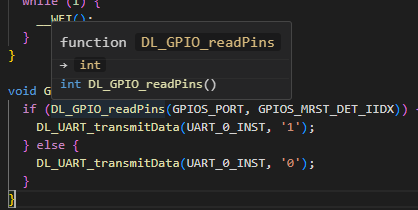
my temporary solution is define static inline as __STATIC_INLINE (really needed?) macro top of main.c file
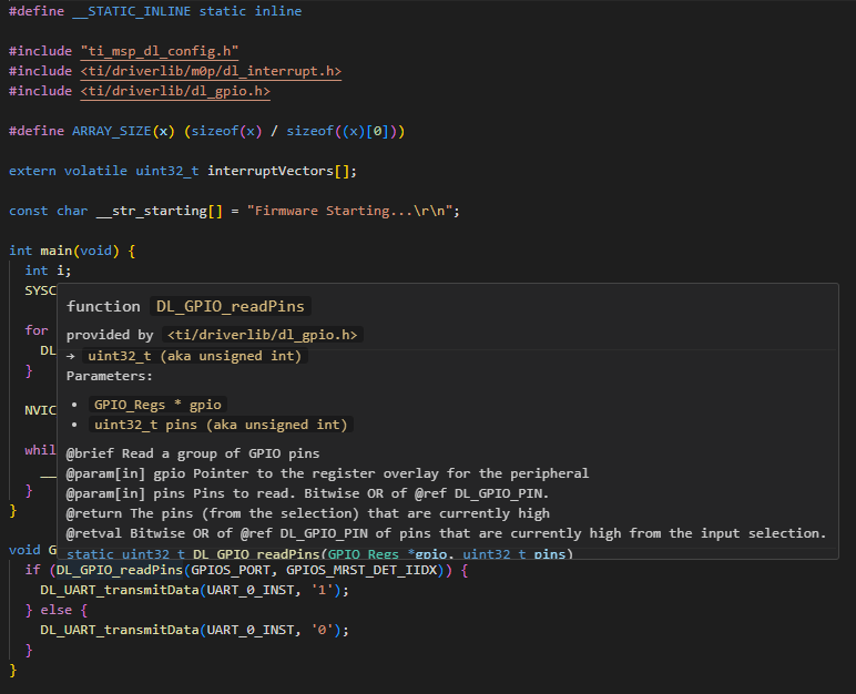
I don't know '__STATIC_INLINE' is 'static inline' but working now
Please fix this
