ADS127L18EVM-PDK: Request for Help Debugging SPI/ADC Code

Part Number: ADS127L18EVM-PDK
Other Parts Discussed in Thread: ADS127L18, MSPM0G3507, TXB-EVM

Good afternoon,

The following repository contains our edited version of the P. Edwards code. In the original Pedwards code he uses two spi peripherals for two data lanes and uses bit banging gpios as the spi controller. However for our application we only require one spi peripheral for data acquisition and the other spi set for the controller, eliminating the need for the bit banging gpios. 


In our implementation:

  • One SPI peripheral is used to receive ADC data.

  • A second SPI data path maps DOUT0 and DCLK for DMA-based data transfer.

  • One SPI controller is used to configure and change the ADC registers.

  • We are not using GPIO bit-banging as in the original P. Edwards implementation.

  • START and RESET are mapped to GPIOs.

  • We are using DOUT0 and DCLK with a single data lane.

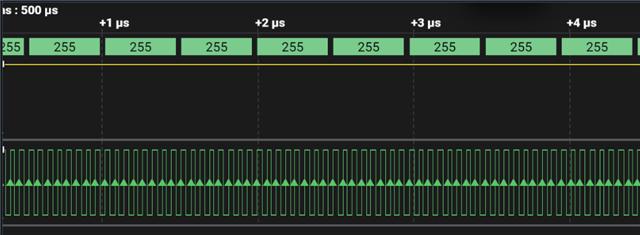
At the moment, we are receiving numbers in gRxPacket, but the channel inputs are unpopulated. Regardless of whether an external input is applied, such as from a function generator, the values remain seemingly random in the 0–255 range.

Additionally, we would like to verify that the SPI controller is functioning correctly. In the main code file, MSPM0xADS127L18.c, I am able to use the single-register read and write functions and see the expected output in the watch variable for the speed check variable. However, I am unable to correctly read the device ID. It appears as 0, even though it should be 6.

Would you be able to help us identify what may be causing this issue, and suggest the best way to verify that SPI communication with the ADS127L18 is working properly?

Updated PEdwards Code (disregard the readme) : https://github.com/JesusPinzon4803/MSPM03507xADS127L18 

Original Edwards Code: https://github.com/TexasInstruments/precision-adc-examples/blob/main/devices/ads127l18/MSPM0_example/README.md 

Thank you.


  • Hello Jesus,

    Which SPI port are you using for conversion data (frame-sync port) and which SPI port are you using for device configuration?  The device configuration port requires SPI mode 1, where SCLK idles low, and the SCLK rising edge launches data and falling edge captures data.

    Also, do you have the MODE pin 54 pulled high with a 3kOhm or lower resistance?  The EVM board uses 100kOhm by default, which is not low enough value to establish a high level on the Mode pin.

    Since this could be a hardware issue in addition to firmware, it is best to start with a logic analyzer and measure the signals.  This will help track down either hardware errors or software.  To start, please capture a full SPI frame for the configuration port, including /CS, SCLK, SDI, and SDO signals.

    Regards,
    Keith Nicholas
    Precision ADC Applications

  • For the frame sync port we are using pins PB17(DOUT0) and PA12(DCLK) and the device configuration spi ports are PB6-9 for CS, SCLK, SDO, SDI

    we have mode set to high on 1.8V for spi programming. 

    we know SCLK is responsible to change the spi mode from 0 to 1 how do we change that, is it through syscfg, or hardware related. The logic analyzer shows that no spi is happening as the CS, SCLK, etc graphs are all flat. For more information on our physical pin connections please look at our syscfg file. Thank you

  • Correction the logic analyzer is able to show some data but it seems unusual. This the the output of the logic analyzer https://github.com/JesusPinzon4803/MSPM03507xADS127L18/blob/main/Screenshot%202026-04-14%20225601.png

  • For the SPI port used to read/write to registers, you need to update the following:

    Phase: Data captured on second clock edge

    Frame size: 16

    /cfs-file/__key/communityserver-discussions-components-files/81/MSPM0_5F00_x_5F00_ADS127L18.syscfg

    Regards,
    Keith

  • Thank you for the response! Unfortunately this did not resolve my issue, would it be possible to get into contact with P-Edwards from TI to aid in our endeavor, or get on a call/real life interaction with a TI employee. 

    during debugging i try two test points for spi communication for the speedcheck, which checks the speed mode of the ADC

        //speedcheck = readSingleRegister(GEN_CFG2_REG_ADDRESS); // retunrns 0!?
        initalizeRegisters(OSR, speed_mode, DP_TDM, DCLK_DIV, ADC_CLK_SEL, ADC_CLK_DIV);
        speedcheck = readSingleRegister(GEN_CFG2_REG_ADDRESS); // does retunrn 6 when speed mode is set to max in earlier code
       
        deviceid = readSingleRegister(DEV_ID_REG_ADDRESS); // should return 6 for L18 but returns 0
    After doing your suggested modifications, the result still outputs a 0 on the device read. Sorry for the headache!
  • Hello Jesus,

    Checking the waveform that you previously sent, it looks like the SPI mode is now correct.  However, I still think this may be a hardware issue.  Please capture a read transaction from one of the registers.  Register CH0_GAN_MSB address 16 should read back 0x40h after reset.  This will be two 16b frames, as shown below:

    This will allow us to confirm the SPI command is correct, and if we do not receive 0x40h, then the ADC is not responding correctly.

    I did notice there was quite a bit of noise on your logic capture.  This could be due to incorrect voltage level set on the logic analyzer (should be 1.8V CMOS logic), or it could be due to high amount of noise/ringing on the digital lines.

    I assume you are using the MSPM0G3507 LaunchPad.  If so, what are you using to voltage level translate from the 3.3V launchpad logic levels to the 1.8V logic required by the ADS127L18EVM?  This logic level translation may be creating noise issues, which is why I ask.

    Regards,
    Keith

  • Hello! Yes we are using a voltage translator (TXB-EVM). We were able to confirm SPI is functioning via a logic analyzer (as it matches the image you provided), however the watch variable is still not updating correctly, is the logic analyzer enough to prove SPI works correctly? Now the main issue is the data lane, DCLK(PA12) and DOUT0(PB17) pins of the ADC. The MCU in the data lane acts as a peripheral taking in the data from the controller, the ADC. In the code I have disabled the previously enabled +/- FS test, thus expecting low/near 0 values since there is no input to our ADC. However when observed from the logic analyzer we see random values, with consistent 255 values. Since the MCU is the peripheral we have it set to SPI mode 0 and capture on rising edge. I have uploaded photos in the github that show the successful SPI and the unexpected data lane values. Additionally I had the voltage translator connections verified by a TI employee.

    Another question, is the intention of this code a continuous collection of data or collection of data in windows. 

    Thank you for your time!

    Here is the github with the photos:

    https://github.com/JesusPinzon4803/MSPM03507xADS127L18 

  • Hello Jesus,

    Yes, it does appear the SPI is now working correctly.  If you want to fully exercise the SPI configuration, you can write a value to any of the offset registers, and then immediately read the value back.  For example:

    Write 0xA5 to register 0x16 and then read it back.  This will be 3 SPI frames, with the following MOSI data:

    0x96A5, write register 0x16 command, register data 0xA5

    0x1600, read register 0x16 command

    0x0000, read register contents

    With the ADS127L18EVM input channels floating, the results should be near 0V, with some noise.  Keep in mind that the output codes can change quite a bit, since small positive values will be near 0x000000h and small negative values will be near 0xFFFFFF due to the two's complement coding of the data.

    The data captured on the DCLK and DOUT lines looks correct.  It does appear that the analyzer is off by 1 clock cycle, but this could be due to your trigger setting.  When capturing the data using the logic analyzer, you should use the FSYNC signal as the SPI chip select and trigger on the FSYNC rising edge.  This will then allow the logic analyzer to correctly interpret the incoming data.  In addition, you can easily tell when a new data conversion cycle begins with each rising edge of FSYNC. 

    Once all channels have been transmitted (24*8=192 DCLK's for 8 channels), the remaining data in a data port frame will be all 1's, or high, when using the ADS127L18EVM.  This is because of the 'daisy-chain' behavior of the data port; once all channel data has been transmitted, then whatever data is on the DINx pin is read and passed through.  In the case of the ADS127L18EVM, the DINx pins are pulled high, and thus 0xFF for all remaining data in a data port frame.

    Based on what you have provided, I think the hardware is now working correctly, including the SPI configuration.  You should be able to capture 512 samples of 24b data over 8 channels using the default settings in the code.

    The intention of this code is to simply show how a standard SPI port can capture the conversion data using a low cost processor.  Most processors cannot directly use the FSYNC signal without additional external logic such as a CPLD.  The MSPM0 does not have enough processing power to continuously capture the data and do something with it.  For short 512 sample bursts, it can be used, but for continuous real-time applications, a much higher performance MCU is required, such as TI's Sitara multi-core application processors, or an FPGA.

    Regards,
    Keith

  • Thank you so much for your patience and aid the issue is now resolved!