Alcor and similarly Aries with dual core the master CPU R4 and slave CPU M3, After power up the M3 is held in reset so JTAG communication is not possible. which is ok to hold the M3 in reset as I am performing most of my tests thru CPU R4.
so I ignore M3 JTAG failure to communicate, or replace the board file such that the M3 is defined by a bypass. however ..
Apparently, writing 0x5 to 0XFFFFFC4 is not enough to Swap R4 RAM to 0x0 Address therefore Flash still stays reside at 0x0? MMU Global Control register need to be Configured MPMENA Therefore need to be set 0xFFFFFFCC to 0x1 to be able to write at 0x0 address
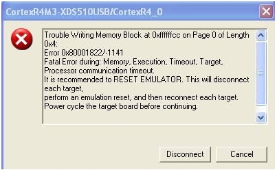
The following message, I am getting Trouble Writing Memory Block 0xFFFFFFCC, only if I cancel that error it seems to allow me to write to RAM at 0x0. How do I override these errors?
that same Trouble Writing Error 0x80001822/-1141 comes any time when remapping Flash à RAM or RAM à FLASH,
Sometimes CPU get into a STALL state and the only way for me to reset is to write 0x0 then 0x1 in 0xffffffCC therefore message above shows up and user need to intervene to cancel the message
Let me know if you have input on these errors and how to avoid STALL.
Best Regards, Ashraf Nabil Texas Instruments-ASP-AEC QIT Team - Product Engineer


