This thread has been locked.

If you have a related question, please click the "Ask a related question" button in the top right corner. The newly created question will be automatically linked to this question.

CCS/TMS320F28335: Plotting ADC Register values gives random output

Part Number: TMS320F28335

Tool/software: Code Composer Studio

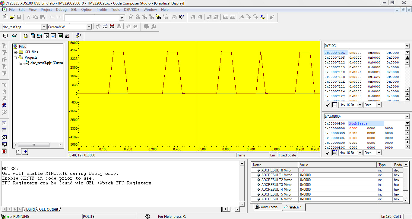
Hello, I am new to CCS. I am using a Texas Instruments Development Board with a TMS320F28335 Control Card. I need to feed rectified sine wave to the ADC of TMS320F28335. I generated code using Matlab. I used CCS4 and CCS 3.3 (on different PCs). Now, when i went to graph utility, there was a 'Starting Address', where i used 0x7111 (I was using ADC Channel B1). I used Real Time Mode. However, the y-axis of the plot was showing data like 6.4*10e4, well over ADC Range (0-4095). The values shown on the graph were random. Then i changed the 'Starting Address' to 0x7108, 0x7109. They also showed similar values on the plot, even when only ADC B1 was connected. I also tried adding 'AdcBuf' to watch window, but CCS 4 was not recognizing it.

How do i confirm that the plot on the graph window belongs to output of ADC Channel B1 ?

The output of ADC should be between 0-4095. Does starting address 0x7011 means the plot would be of result of ADC B1 only or is it my misunderstanding?

I have tried almost everything i could, but in vain. Kindly instruct me on how to proceed (CCS4 or CCS3.3). I shall be grateful for any assistance.

Thank You !

  • Hi,

    Unfortunately there is not much information to et a precise assessment of the root cause. When using graph, the parameters used, the address and the place where the breakpoint is set are critical for a proper display.

    An example on how to properly set up the graph to display a 12-bit ADC and configure a breakpoint to read the ADC data register is shown at the page below:
    processors.wiki.ti.com/.../Graph_Visualization_for_MSP430

    Keep in mind that, depending on the device, reading the ADC register once may clear its value - in this case you can either copy the value to a variable or create a buffer to graph a number of values by setting the parameter "Acquisition Buffer Size".

    At last, if you are still using CCSv4 I must tell you that many bugs were fixed in newer releases of CCS - some of them critical to a proper display.

    I would strongly suggest you to try a newer version and see if you get better results.

    Hope this helps,
    Rafael
  • Hello, thank you for your earlier reply.

    I made a program in which Pulses of period 2 seconds with 50% duty ratio were being generated and obtained at GPIO 27. I connected GPIO 27 pin to ADC A4 pin to verify the graph utility in CCS. I generated the code from MATLAB. I used Real Time Mode in CCS. I did not set any breakpoints manually. I added ADCRESULT0 Mirror to Watch Window.

    I then plotted ADCRESULT0 Mirror using Graph with starting address 0x0B00. 

    The graph property dialog is shown in the attached pic:

     When GPIO 27 was connected to ADC A4, the following output was obtained:

    However, when GPIO 27 was disconnected from ADC A4, the ADC Output went high and stayed so as shown below.

    The graph obtained for same code and same properties in CCS 4 is shown:

    Kindly answer my following queries:

    1. Why when the GPIO 27 pin is disconnected from ADC A4 pin, the ADC output goes high? Shouldn't it go low and near zero since there is no input to it?
    2. Why is the graph showing trapezoidal pulses rather than the expected square pulses?
    3. The unit of the horizontal axis on these graphs is seconds. The time period of the pulses should be 2 seconds. Observing the values of ADCRESULT0 Mirror in watch window (with continuous refresh) also shows a time period of 2 seconds. However, in the graph the time period is much less (approx 0.2 sec). The time period in the graph also seemed to vary with changing some properties of the graph. How to obtain correct time period in the graph window?

    I appreciate you taking out time to respond to my queries. I shall be grateful. Thank You!

  • 1 The input will float, and unless you have a pulldown, can read any voltage.
    2. Your timing is probably not right. I think we need to see the code.
  • Hi Kieth, 
    The code has been generated using Embedded Coder in MATLAB SIMULINK. There is a pulse generator giving output to GPIO 27. There is ADC A4 giving
    output to GPIO 32. After running the code, i am manually connecting GPIO 27 with ADC A4, and monitoring ADC values in CCS. Why is the time period and
    shape of pulses wrong in Graph Window but right in Watch Window. Thank You!


    /* * File: dsc_test3.c * * Code generated for Simulink model 'dsc_test3'. * * Model version : 1.2 * Simulink Coder version : 8.2 (R2012a) 29-Dec-2011 * TLC version : 8.2 (Dec 29 2011) * C/C++ source code generated on : Tue May 02 10:05:51 2017 * * Target selection: idelink_ert.tlc * Embedded hardware selection: Texas Instruments->C2000 * Code generation objectives: Unspecified * Validation result: Not run */ #include "dsc_test3.h" #include "dsc_test3_private.h" /* Block signals (auto storage) */ BlockIO_dsc_test3 dsc_test3_B; /* Block states (auto storage) */ D_Work_dsc_test3 dsc_test3_DWork; /* Real-time model */ RT_MODEL_dsc_test3 dsc_test3_M_; RT_MODEL_dsc_test3 *const dsc_test3_M = &dsc_test3_M_; static void rate_monotonic_scheduler(void); /* * Set which subrates need to run this base step (base rate always runs). * This function must be called prior to calling the model step function * in order to "remember" which rates need to run this base step. The * buffering of events allows for overlapping preemption. */ void dsc_test3_SetEventsForThisBaseStep(boolean_T *eventFlags) { /* Task runs when its counter is zero, computed via rtmStepTask macro */ eventFlags[1] = ((boolean_T)rtmStepTask(dsc_test3_M, 1)); } /* rate_monotonic_scheduler */ static void rate_monotonic_scheduler(void) { /* Compute which subrates run during the next base time step. Subrates * are an integer multiple of the base rate counter. Therefore, the subtask * counter is reset when it reaches its limit (zero means run). */ (dsc_test3_M->Timing.TaskCounters.TID[1])++; if ((dsc_test3_M->Timing.TaskCounters.TID[1]) > 999) {/* Sample time: [0.1s, 0.0s] */ dsc_test3_M->Timing.TaskCounters.TID[1] = 0; } } /* Model step function for TID0 */ void dsc_test3_step0(void) /* Sample time: [0.0001s, 0.0s] */ { { /* Sample time: [0.0001s, 0.0s] */ rate_monotonic_scheduler(); } /* DiscretePulseGenerator: '<Root>/Pulse Generator' */ dsc_test3_B.PulseGenerator = ((real_T)dsc_test3_DWork.clockTickCounter < dsc_test3_P.PulseGenerator_Duty) && (dsc_test3_DWork.clockTickCounter >= 0L) ? dsc_test3_P.PulseGenerator_Amp : 0.0; if ((real_T)dsc_test3_DWork.clockTickCounter >= dsc_test3_P.PulseGenerator_Period - 1.0) { dsc_test3_DWork.clockTickCounter = 0L; } else { dsc_test3_DWork.clockTickCounter++; } /* End of DiscretePulseGenerator: '<Root>/Pulse Generator' */ /* S-Function Block: <Root>/Digital Output 27 (c280xgpio_do) */ { GpioDataRegs.GPASET.bit.GPIO27 = (dsc_test3_B.PulseGenerator != 0); GpioDataRegs.GPACLEAR.bit.GPIO27 = !(dsc_test3_B.PulseGenerator != 0); } } /* Model step function for TID1 */ void dsc_test3_step1(void) /* Sample time: [0.1s, 0.0s] */ { /* S-Function Block: <Root>/ADC (c280xadc) */ { AdcRegs.ADCTRL2.bit.RST_SEQ1 = 1; /* Reset SEQ1 module*/ AdcRegs.ADCST.bit.INT_SEQ1_CLR = 1;/*clear INT sequencer*/ AdcRegs.ADCTRL2.bit.SOC_SEQ1 = 1; /* Software Trigger*/ while (AdcRegs.ADCST.bit.INT_SEQ1 == 0) { } /*Wait for Sequencer INT bit to clear */ asm(" RPT #11 || NOP"); dsc_test3_B.ADC = (AdcRegs.ADCRESULT0) >> 4; } /* S-Function Block: <Root>/Digital Output 32 (c280xgpio_do) */ { GpioDataRegs.GPBSET.bit.GPIO32 = (dsc_test3_B.ADC != 0); GpioDataRegs.GPBCLEAR.bit.GPIO32 = !(dsc_test3_B.ADC != 0); } } void dsc_test3_step(int_T tid) { switch (tid) { case 0 : dsc_test3_step0(); break; case 1 : dsc_test3_step1(); break; default : break; } } /* Model initialize function */ void dsc_test3_initialize(void) { /* Registration code */ /* initialize real-time model */ (void) memset((void *)dsc_test3_M, 0, sizeof(RT_MODEL_dsc_test3)); /* block I/O */ (void) memset(((void *) &dsc_test3_B), 0, sizeof(BlockIO_dsc_test3)); /* states (dwork) */ (void) memset((void *)&dsc_test3_DWork, 0, sizeof(D_Work_dsc_test3)); /* Start for S-Function (c280xadc): '<Root>/ADC' */ InitAdc(); config_ADC_A (0U, 3U, 0U, 0U, 0U); /* Start for S-Function (c280xgpio_do): '<Root>/Digital Output 32' */ EALLOW; GpioCtrlRegs.GPBMUX1.all &= 4294967292U; GpioCtrlRegs.GPBDIR.all |= 1U; EDIS; /* Start for DiscretePulseGenerator: '<Root>/Pulse Generator' */ dsc_test3_DWork.clockTickCounter = 0L; /* Start for S-Function (c280xgpio_do): '<Root>/Digital Output 27' */ EALLOW; GpioCtrlRegs.GPAMUX2.all &= 4282384383U; GpioCtrlRegs.GPADIR.all |= 134217728U; EDIS; } /* Model terminate function */ void dsc_test3_terminate(void) { /* (no terminate code required) */ } /* * File trailer for generated code. * * [EOF] */