This thread has been locked.

If you have a related question, please click the "Ask a related question" button in the top right corner. The newly created question will be automatically linked to this question.

CCS: Piccolo F28027, shift count too large

Other Parts Discussed in Thread: TMS320F28027

Tool/software: Code Composer Studio

Hi,

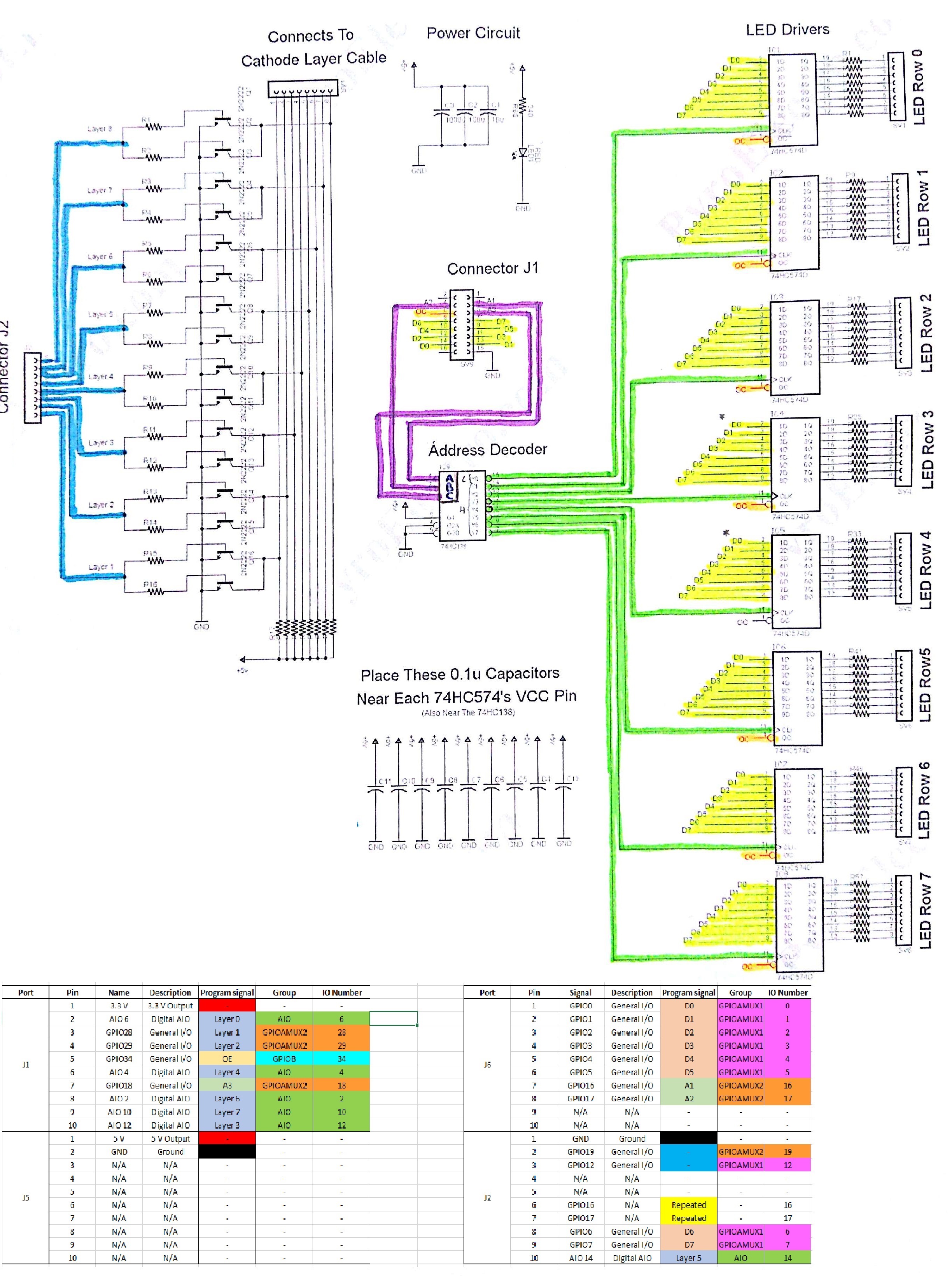
I am working in a project with a 8x8x8 cube led with 74hc138 and 74hc574 to control the ignition of the LEDs.

The main problem is that the code part in the interruption wich manages the inputs for the 74hc138 , is not working fine.

The following code is in charge of this part:

int i;

for (i=0;i<8;i++)

{

      GpioDataRegs.GPADAT.all=cube[current_layer][i];

      GpioDataRegs.GPADAT.all=(GpioDataRegs.GPADAT.all & 0x00000011)|((0x07 & (i+1))<<16);

}

When the code is compiled, a warning appears:

#64-D shift count is too large

The goal of that code part is to manage all the combinations for the 74hc138 inputs (A1,A2,A3) as I said before. These inputs are located at GPIO16,17 and 18.

When I am debugging the code, at this pins only I can see a LOW signal at all of them.

PS: sorry for the format used, I am posting with the smartphone.

Thanks in advance

Best Regards,

Miguel

  • Miguel Valera said:
          GpioDataRegs.GPADAT.all=(GpioDataRegs.GPADAT.all & 0x00000011)|((0x07 & (i+1))<<16);

    On a C2800 device the size of int is 16-bits. The sub-expression ((0x07 & (i+1))<<16) is of type int, so the compiler is correctly warning that the left-shift count of 16 applied to an int is too large and will result in a sub-expression value of zero.

    You need to cast the sub-expression to produce a 32-bit result. E.g. by changing the code to:

        int i;
    
        for (i=0;i<8;i++)
        {
              GpioDataRegs.GPADAT.all=cube[current_layer][i];
              GpioDataRegs.GPADAT.all=(GpioDataRegs.GPADAT.all & 0x00000011)|((0x07 & ((Uint32)i+1))<<16);
        }

    I chose a cast to type Uint32 since that is the type of GpioDataRegs.GPADAT.all

  • Hi Chester,

    Thanks for your quick answer. It was very useful for me.

    I have another question, maybe you know the answer.

    When I am debugging the code, I cannot obtain a stable HIGH output in the output pins.

    The code part in charge of that is the samethan before:

    GpioDataRegs.GPADAT.all=0x000000FF;

    But if I see the GPIOs in the watch expression windows,  only GPIO 1 and 4 are allways in a HIGH output, threst of GPIOs are varying, the same occurs when I see the pins through an oscilloscope.

    Thanks in advance,

    Regards,

    Miguel

  • Miguel Valera said:
    But if I see the GPIOs in the watch expression windows,  only GPIO 1 and 4 are allways in a HIGH output, threst of GPIOs are varying, the same occurs when I see the pins through an oscilloscope.

    I suspect a hardware problem, such as trying to source a higher current than the TMS320F28027 GPIO pins can supply.

    Can you show a schematic of your hardware?

  • Sure!

    The original project is using arduino, but i am trying to adapt to Piccolo F28027.

  • What is the value of the resistors between the Layer0 .. Layer7 GPIOs and the base of the 2N2222 transistors?

  • All of them are 100 ohm resistors
  • Miguel Valera said:
    All of them are 100 ohm resistors

    Each GPIO for the Layer1 .. Layer 8 signals is connected with 100 ohm resistors the base of two 2N2222 transistors in parallel. 

    If the 2N2222 Base Emitter Saturation Voltage is 0.6, the minimum specified in the datasheet, then a GPIO high will try and source (3.3 - 0.6) / (100 / 2) = 54 mA.

    If the 2N2222 Base Emitter Saturation Voltage is 2.6, the minimum specified in the datasheet, then a GPIO high will try and source (3.3 - 2.6) / (100 / 2) = 14 mA.

    The TMS320F28027 datasheet shows the maximum current which can be sourced for a GPIO high is 4 mA or 8 mA, depending upon the pin:

    Trying to source more current from a GPIO high than the device can support will result in an indeterminate output voltage and may damage the TMS320F28027.

    Rather than trying to get the TMS320F28027 GPIOs to directly drive the base of the 2N2222 transistors suggest you need to add an intermediate device which can source the required current to drive the base of the 2N2222 transistors. 

  • Thank you very much for the information.

    But my main problem is not with the GPIOs which manage the layers, it is with the data pins (D0-D7), which go directly to the 74hc574.

    Is it probably the problem that you said before affects to these outputs?

  • Miguel Valera said:
    But my main problem is not with the GPIOs which manage the layers, it is with the data pins (D0-D7), which go directly to the 74hc574.

    OK, what is the content of the cube array?

    Is the cube array supposed to contain the values of the data pins D0-D7 and the layer signals layer0 .. layer7 ?

    The code from the original post was the following:

    int i;
    
    for (i=0;i<8;i++)
    {
         GpioDataRegs.GPADAT.all=cube[current_layer][i];
         GpioDataRegs.GPADAT.all=(GpioDataRegs.GPADAT.all & 0x00000011)|((0x07 & (i+1))<<16);
    }

    The first assignment to GpioDataRegs.GPADAT.all could well be setting the value of the D0 .. D7 and layer0 .. layer7 signals, but the second assignment to GpioDataRegs.GPADAT.all will only keep the value of data bits D1 and D4 due to the mask (GpioDataRegs.GPADAT.all & 0x00000011). When the code is running that could cause the D0, D2-D3,D5-D7 and layer0 .. layer7 signals to fluctuate, and the signals may be zero when stopped in the debugger (depending where halted).

    Also, since the the output from the 74HC138 address decoder are used to clock the 74HC574 devices the program needs to control the order the GPIO outputs are changed to ensure there are no unwanted glitches on the 74HC574 clock input which cause incorrect updates to the LED rows.

  • The content for the cube array is the Z and Y coordenates (cube[Z][Y]), these coordenates are the layers and rows, and the information content when for example is assigned 0xFF, it means that all the row has to be active (X axle).

    With your explanation, it makes sense for me that the mask is wrong, since it is not keeping the D0-D7 information, it would be 0xFF.

    "Also, since the the output from the 74HC138 address decoder are used to clock the 74HC574 devices the program needs to control the order the GPIO outputs are changed to ensure there are no unwanted glitches on the 74HC574 clock input which cause incorrect updates to the LED rows."

    Respect of this, the order to control which clock is active, I use this line:

    GpioDataRegs.GPADAT.all=(GpioDataRegs.GPADAT.all & 0x00000011)|((0x07 & (i+1))<<16);

    In order to provoke a rising edge in every CLK of the 74hc574. do you think this is wrong?

  • Miguel Valera said:
    Respect of this, the order to control which clock is active, I use this line:
    GpioDataRegs.GPADAT.all=(GpioDataRegs.GPADAT.all & 0x00000011)|((0x07 & (i+1))<<16);

    In order to provoke a rising edge in every CLK of the 74hc574. do you think this is wrong?

    GPIO bits 18..16 map to the address bits A2..A0 on the 74HC138, where changing the address bits A2..A0 will cause clock pulses to the 74HC574 row driver latches.

    Inside the for loop there two two statements which write to the address bits A2..A0. The first statement will set A2..A0 to all zeros and the second will cycle around the different A2..A0 combinations:

    for (i=0;i<8;i++)
    {
          GpioDataRegs.GPADAT.all=cube[current_layer][i];
          GpioDataRegs.GPADAT.all=(GpioDataRegs.GPADAT.all & 0x00000011)|((0x07 & ((Uint32)i+1))<<16);
    }

    I.e. the following sequence:

    i write to GpioDataRegs.GPDAT.all A2..A0 change to 74HC574 clock(s)
    0
    cube[current_layer][i]
    0 row 0 is low
    0
    (GpioDataRegs.GPADAT.all & 0x00000011)|((0x07 & ((Uint32)i+1))<<16)
    1

    row 0 goes high
    row 1 goes low

    1
    cube[current_layer][i]
    0 row 0 goes low
    row 1 goes high
    1
    (GpioDataRegs.GPADAT.all & 0x00000011)|((0x07 & ((Uint32)i+1))<<16)
    2 row 0 goes high
    row 2 goes low
    2
    cube[current_layer][i]
    0 row 0 goes low
    row 2 goes high
    2
    (GpioDataRegs.GPADAT.all & 0x00000011)|((0x07 & ((Uint32)i+1))<<16)
    3 row 0 goes high
    row 3 goes low
    3
    cube[current_layer][i]
    0 row 0 goes low
    row 3 goes high
    3
    (GpioDataRegs.GPADAT.all & 0x00000011)|((0x07 & ((Uint32)i+1))<<16)
    4 row 0 goes high
    row 4 goes low
    4
    cube[current_layer][i]
    0 row 0 goes low
    row 4 goes high
    4
    (GpioDataRegs.GPADAT.all & 0x00000011)|((0x07 & ((Uint32)i+1))<<16)
    5

    row 0 goes high
    row 5 goes low

    5
    cube[current_layer][i]
    0 row 0 goes low
    row 5 goes high
    5
    (GpioDataRegs.GPADAT.all & 0x00000011)|((0x07 & ((Uint32)i+1))<<16)
    6 row 0 goes high
    row 6 goes low
    6
    cube[current_layer][i]
    0 row 0 goes low
    row 6 goes high
    6
    (GpioDataRegs.GPADAT.all & 0x00000011)|((0x07 & ((Uint32)i+1))<<16)
    7 row 0 goes high
    row 7 goes low
    7
    cube[current_layer][i]
    0 row 0 goes low
    row 7 goes high
    7
    (GpioDataRegs.GPADAT.all & 0x00000011)|((0x07 & ((Uint32)i+1))<<16)
    0 no change
    0
    cube[current_layer][i]
    0 no change

    The issues with the above are:

    a) There are multiple rising clock edges on 74HC574 row 0 clock, which means unwanted changes to the row 0 LEDs.

    b) The data bits D7..D0 inputs to the 74HC574's change together with the A2..A0 bits which drive the 74HC574's clock, which could mean the 74HC574 setup / hold time is violated leading to indeterminate row LEDs outputs.

    c) The sequencing of changes to the A2..A0 address bits means more than one bit changes at a time, which may lead to glitches from the 74HC138 leading to unwanted changes to the row LEDs if the glitches are fast enough to generate a clock edge on the 74HC574's. To avoid that recommend causing the A2..A0 address bits to change as a Gray code so that only one bit changes at a time.

    I would be helpful to produce a timing diagram of how the code changes all the output for the LED cube to check that the sequence is correct, also including the layer drivers. I assume the refresh cycle needs to alternate around each layer in turn.

  • Thank so much Chester, your help was and is  very useful for me.

    I changed the mask because it was wrong, it was doing the D0-D7 data bits changed with the A2-A0 codification.

    Now it seems working fine.

    Respect of the gray code codification, I do not know how to do that.

    Sorry for the delay of my answer.

  • Miguel Valera said:
    Respect of the gray code codification, I do not know how to do that.

    For the gray code modification I mean that instead of cycling through the A2-A0 address bits in the order 0, 1, 2, 3, 4, 5, 6, 7 instead use the order 0, 1, 3, 2, 6, 7, 5, 4.

    The significance of changing the A2-A0 address bits in a gray code order is that only one bit changes at a time to remove the possibility of getting glitches out of the 74HC138 address decoder if multiple address bits change at the same time. Where glitches out of the 74HC138 may result in an incorrect row 74HC574 being clocked with data.

  • Thanks Chester, all your information is very useful for me !