


Part Number: ADS1274EVM-PDK
Other Parts Discussed in Thread: ADS1274
Tool/software: Code Composer Studio
Hi! I'd like to present two problems I've experienced while working with acquiring data from the ADS1274EVM on the 1294XL Launchpad. As a background, I'd like to provide the following information:
- I am attempting to read multiple Channels in the ADS1274 using the 1294XL ICDI, without using the MMB0
- The analog input is a sine wave, and the function generator is connected to all of the analog inputs, which is what I'm looking for in the CCS graph
- In order to start simple, I start out using just two channels. One channel shows the expected sine wave, and the other channel shows half a sine wave, then complete garbage. Like this
//This code contains the SPI with the timer and interrupt

#define INPUT_VECTOR_SIZE 100

uint32_t ui32SysClkFreq;                          //Clock frequency (Also can be called by SysClockFreqGet())
uint32_t ui32Period;                              //Number of Clock cycles before the next interrupt is sent
uint16_t DummyData = 0x0000;
uint32_t counter = 0;
uint16_t pui16DataRx0[INPUT_VECTOR_SIZE] = {0x0000};    //Create Empty Input Vector for Channel 1
uint16_t pui16DataRx1[INPUT_VECTOR_SIZE] = {0x0000};    //Create Empty Input Vector for Channel 2
uint16_t pui16DataRx2[INPUT_VECTOR_SIZE] = {0x0000};    //Create Empty Input Vector for Channel 3
uint16_t pui16DataRx3[INPUT_VECTOR_SIZE] = {0x0000};    //Create Empty Input Vector for Channel 4
uint32_t pui32DataRxBuffer[7]            = {0x0000};    //Rx buffer, will be Rearranged in DRDY ISR

void GPIOPortFIntHandler(void);

int main(void)
{
    //Configure the Clock
    ui32SysClkFreq = SysCtlClockFreqSet((SYSCTL_XTAL_25MHZ | SYSCTL_OSC_MAIN | SYSCTL_USE_PLL | SYSCTL_CFG_VCO_480), 120000000);


    //Enable Associated GPIO and SSI Peripherals For SSI1
    SysCtlPeripheralEnable(SYSCTL_PERIPH_SSI1);
    SysCtlPeripheralEnable(SYSCTL_PERIPH_GPIOB);
    SysCtlPeripheralEnable(SYSCTL_PERIPH_GPIOE);


    //Configure and Activate Pins for SSI (Pg 743 of Datasheet for reference)
    GPIOPinConfigure(GPIO_PB5_SSI1CLK);
    GPIOPinConfigure(GPIO_PE4_SSI1XDAT0);
    GPIOPinConfigure(GPIO_PE5_SSI1XDAT1);
    GPIOPinTypeSSI(GPIO_PORTB_BASE,GPIO_PIN_5);
    GPIOPinTypeSSI(GPIO_PORTE_BASE,GPIO_PIN_4|GPIO_PIN_5);

    //Configure Constant GPIO Pins (SYNC, MODE and FORMAT Pins)
    SysCtlPeripheralEnable(SYSCTL_PERIPH_GPIOK);
    GPIOPinTypeGPIOOutput(GPIO_PORTK_BASE, GPIO_PIN_5 | GPIO_PIN_4 | GPIO_PIN_3
                                         | GPIO_PIN_2 | GPIO_PIN_1 | GPIO_PIN_0 );
    GPIOPinWrite(GPIO_PORTK_BASE, 0x3F, 0x20);                      // /SYNC: 1b'1; FORMAT: 3b'000; MODE: 2b'00

    // Pin F4 setup for DRDY-Inverse
    SysCtlPeripheralEnable(SYSCTL_PERIPH_GPIOF);        // Enable port F
    GPIOPinTypeGPIOInput(GPIO_PORTF_BASE, GPIO_PIN_0);  // Init PF0 as input

    // Interrupt setup
    GPIOIntDisable(GPIO_PORTF_BASE, GPIO_PIN_0);                // Disable interrupt for PF0 (in case it was enabled)
    GPIOIntTypeSet(GPIO_PORTF_BASE, GPIO_PIN_0, GPIO_FALLING_EDGE);                          // Configure PF0 for falling edge trigger
    GPIOIntClear(GPIO_PORTF_BASE, GPIO_PIN_0);                  // Clear pending interrupts for PF0
    GPIOIntRegister(GPIO_PORTF_BASE, GPIOPortFIntHandler);      // Register ISR for port F
    GPIOIntEnable(GPIO_PORTF_BASE, GPIO_PIN_0);                 // Enable interrupt for PF0


    //Configure SSI: DAC Reads on Rising Edge (Phase = 1), Idle Mode is High (Polarity = 1)
    SSIConfigSetExpClk(SSI1_BASE, ui32SysClkFreq, SSI_FRF_MOTO_MODE_0, SSI_MODE_MASTER, 20000000, 16);
    SSIEnable(SSI1_BASE);
    //Continue
    while(1){}
}


//Interrupt Service Routine (ISR) or Interrupt Handler
void GPIOPortFIntHandler(void)
{

        //Clear the GPIO interrupt
        GPIOIntClear(GPIO_PORTF_BASE, GPIO_INT_PIN_0);


        //Fill the buffer elements one by one; collect 64 bits
        SSIDataPut(SSI1_BASE, DummyData);
        SSIDataGet(SSI1_BASE,&pui32DataRxBuffer[0]);             //Get first 16 bits [111:96]
        SSIDataPut(SSI1_BASE, DummyData);
        SSIDataGet(SSI1_BASE,&pui32DataRxBuffer[1]);             //Get second  16 bits [95:80]
        SSIDataPut(SSI1_BASE, DummyData);
        SSIDataGet(SSI1_BASE,&pui32DataRxBuffer[2]);             //Get third 16 bits [79:64]
        SSIDataPut(SSI1_BASE, DummyData);
        SSIDataGet(SSI1_BASE,&pui32DataRxBuffer[3]);             //Get fourth  16 bits [63:48]
        //SSIDataPut(SSI1_BASE, DummyData);
        //SSIDataGet(SSI1_BASE,&pui32DataRxBuffer[4]);             //Get fifth 16 bits [47:32]
        //SSIDataPut(SSI1_BASE, DummyData);
        //SSIDataGet(SSI1_BASE,&pui32DataRxBuffer[5]);             //Get sixth 16 bits [31:16]
        //SSIDataPut(SSI1_BASE, DummyData);
        //SSIDataGet(SSI1_BASE,&pui32DataRxBuffer[6]);             //Get seventh 16 bits [15: 0]

        //Consolidate and concatenate the elements to get Channel 1 and 2
        pui16DataRx0[counter] = ((uint16_t)(pui32DataRxBuffer[0]) << 1) | ((uint16_t)(pui32DataRxBuffer[1]) >> 15);
        pui16DataRx1[counter] = ((uint16_t)(pui32DataRxBuffer[1]) << 9) | ((uint16_t)(pui32DataRxBuffer[2]) >>  7);
        //pui16DataRx2[counter] = ((uint16_t)(pui32DataRxBuffer[3]) << 1) | ((uint16_t)(pui32DataRxBuffer[4]) >> 15);
        //pui16DataRx3[counter] = ((uint16_t)(pui32DataRxBuffer[4]) << 9) | ((uint16_t)(pui32DataRxBuffer[5]) >>  7);

        //Counter Update
        if(counter < INPUT_VECTOR_SIZE - 1) {counter++;}        //Increment Counter as long as it's below 4999
        else{counter = 0;}                                      //Reset Counter to Zero if it is 4999
        while(SSIBusy(SSI1_BASE)){}

}
Output for pui16DataRx0:

Output for pui16DataRx1:
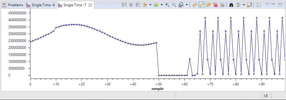
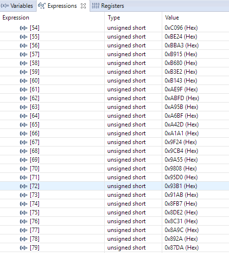
I also checked the expression values for the elements of pui16DataRx1 from element 50 to 100, and it looks pretty okay (like a sine wave), unlike what I see on the graph. It's given below. Can anyone suggest what could be wrong here?
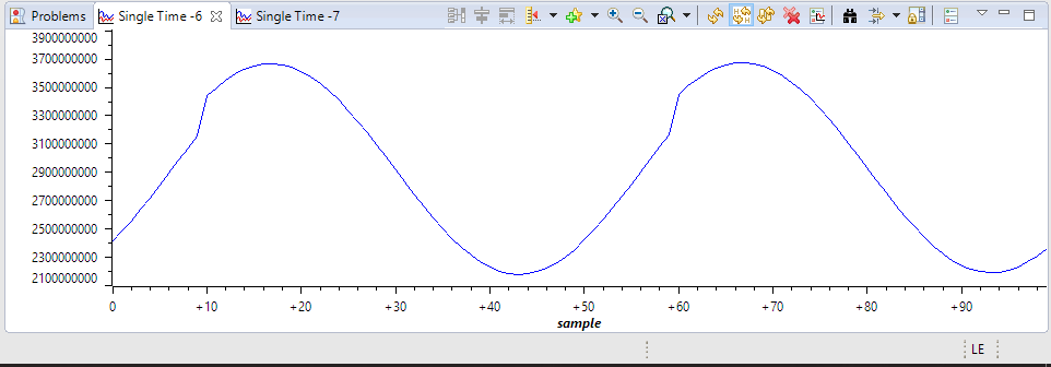
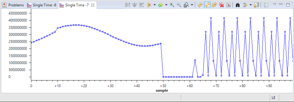
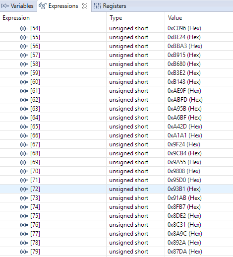
Another issue I've been having is that when I turn on all 4 channels and I uncomment all the commented sections in the code above to accommodate the extra data, I get garbage values in my input buffer (looks like noise on the graphing function, and the hex values on the expression viewer don't look any more meaningful).
I'd appreciate anyone's help on the issues presented above. Please let me know if more information is required, I'll provide it asap.
Regards,
Stefan
