This thread has been locked.

If you have a related question, please click the "Ask a related question" button in the top right corner. The newly created question will be automatically linked to this question.

CCS/TMS320F28069: Code Composer Studio V8

Part Number: TMS320F28069
Other Parts Discussed in Thread: LAUNCHXL-F28069M,

Tool/software: Code Composer Studio

Sir, Thanks In Advance.

I have down loaded Example_2806xAdcSoc, and I have Launchpad LAUNCHXL-F28069M.

I compiled and ran program in debug mode successfully.

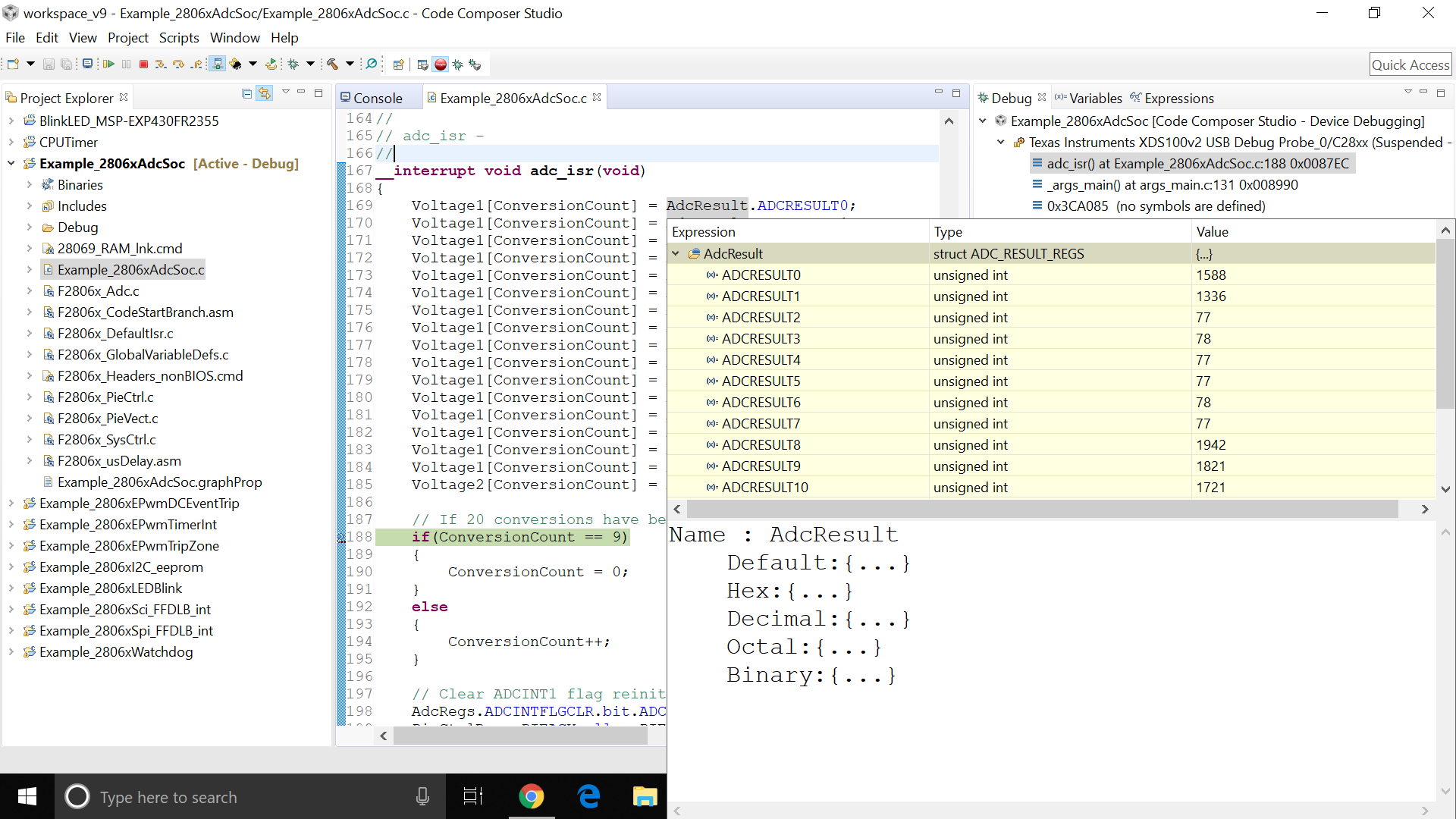
I shorted, J1-PIN-1 (+3.3V) and  J3-PIN-25 (ADCINA2), Expecting ADCResult1 will show Value 0xFFFFh.

I did not  get ADCResult1 = 0xFFFFh.

I tried to see all ADCResult0 To ADCResult15, and I got none of them equal to or near by value 0xFFFFh, by pacing cursor over line,

Voltage1[ConversionCount] = AdcResult.ADCRESULT0; and word ADCRESULT0 To ADCRESULT15.

My Program Example_2806xAdcSoc.C is as follows.

//###########################################################################
//
// FILE:   Example_2806xAdcSoc.c
//
// TITLE:  ADC Start of Conversion Example
//
//! \addtogroup f2806x_example_list
//! <h1> ADC Start of Conversion (adc_soc)</h1>
//! 
//! This ADC example uses ePWM1 to generate a periodic ADC SOC - ADCINT1.
//! Two channels are converted, ADCINA4 and ADCINA2.
//! 
//! \b Watch \b Variables \n
//! - Voltage1[10]    - Last 10 ADCRESULT0 values
//! - Voltage2[10]    - Last 10 ADCRESULT1 values
//! - ConversionCount - Current result number 0-9
//! - LoopCount       - Idle loop counter
//
//###########################################################################
// $TI Release: F2806x Support Library v2.04.00.00 $
// $Release Date: Mon May 27 06:46:38 CDT 2019 $
// $Copyright:
// Copyright (C) 2009-2019 Texas Instruments Incorporated - http://www.ti.com/
//
// Redistribution and use in source and binary forms, with or without 
// modification, are permitted provided that the following conditions 
// are met:
// 
//   Redistributions of source code must retain the above copyright 
//   notice, this list of conditions and the following disclaimer.
// 
//   Redistributions in binary form must reproduce the above copyright
//   notice, this list of conditions and the following disclaimer in the 
//   documentation and/or other materials provided with the   
//   distribution.
// 
//   Neither the name of Texas Instruments Incorporated nor the names of
//   its contributors may be used to endorse or promote products derived
//   from this software without specific prior written permission.
// 
// THIS SOFTWARE IS PROVIDED BY THE COPYRIGHT HOLDERS AND CONTRIBUTORS 
// "AS IS" AND ANY EXPRESS OR IMPLIED WARRANTIES, INCLUDING, BUT NOT 
// LIMITED TO, THE IMPLIED WARRANTIES OF MERCHANTABILITY AND FITNESS FOR
// A PARTICULAR PURPOSE ARE DISCLAIMED. IN NO EVENT SHALL THE COPYRIGHT 
// OWNER OR CONTRIBUTORS BE LIABLE FOR ANY DIRECT, INDIRECT, INCIDENTAL, 
// SPECIAL, EXEMPLARY, OR CONSEQUENTIAL DAMAGES (INCLUDING, BUT NOT 
// LIMITED TO, PROCUREMENT OF SUBSTITUTE GOODS OR SERVICES; LOSS OF USE,
// DATA, OR PROFITS; OR BUSINESS INTERRUPTION) HOWEVER CAUSED AND ON ANY
// THEORY OF LIABILITY, WHETHER IN CONTRACT, STRICT LIABILITY, OR TORT 
// (INCLUDING NEGLIGENCE OR OTHERWISE) ARISING IN ANY WAY OUT OF THE USE 
// OF THIS SOFTWARE, EVEN IF ADVISED OF THE POSSIBILITY OF SUCH DAMAGE.
// $
//###########################################################################
//
// Included Files
//
#include "DSP28x_Project.h"     // Device Headerfile and Examples Include File
//
// Function Prototypes
//
__interrupt void adc_isr(void);
void Adc_Config(void);
//
// Globals
//
Uint16 LoopCount;
Uint16 ConversionCount;
Uint16 Voltage1[10];
Uint16 Voltage2[10];
//
// Main
// 
void main(void)
{
    // Step 1. Initialize System Control:
    // PLL, WatchDog, enable Peripheral Clocks
    // This example function is found in the F2806x_SysCtrl.c file.
    //
    InitSysCtrl();
    // Step 2. Initialize GPIO:
    // This example function is found in the F2806x_Gpio.c file and
    // illustrates how to set the GPIO to it's default state.
    // InitGpio();  // Skipped for this example
    // Step 3. Clear all interrupts and initialize PIE vector table:
    // Disable CPU interrupts
    DINT;
    // Initialize the PIE control registers to their default state.
    // The default state is all PIE interrupts disabled and flags
    // are cleared.
    // This function is found in the F2806x_PieCtrl.c file.
    InitPieCtrl();
    // Disable CPU interrupts and clear all CPU interrupt flags:
    IER = 0x0000;
    IFR = 0x0000;
    // Initialize the PIE vector table with pointers to the shell Interrupt Service Routines (ISR).
    // This will populate the entire table, even if the interrupt
    // is not used in this example.  This is useful for debug purposes.
    // The shell ISR routines are found in F2806x_DefaultIsr.c.
    // This function is found in F2806x_PieVect.c.
    InitPieVectTable();
    // Interrupts that are used in this example are re-mapped to
    // ISR functions found within this file.
    EALLOW;  // This is needed to write to EALLOW protected register
    PieVectTable.ADCINT1 = &adc_isr;
    EDIS;    // This is needed to disable write to EALLOW protected registers
    // Step 4. Initialize all the Device Peripherals:
    // This function is found in F2806x_InitPeripherals.c
    // InitPeripherals(); // Not required for this example
    // For this example,Initialize ADC
    InitAdc();
    AdcOffsetSelfCal();
    // Step 5. User specific code, enable interrupts:
    // Enable ADCINT1 in PIE
    PieCtrlRegs.PIEIER1.bit.INTx1 = 1; // Enable INT 1.1 in the PIE
    IER |= M_INT1;    // Enable CPU Interrupt 1
    EINT;             // Enable Global interrupt INTM
    ERTM;             // Enable Global real time interrupt DBGM
    LoopCount = 0;
    ConversionCount = 0;
    // Configure ADC
    EALLOW;
    AdcRegs.ADCCTL2.bit.ADCNONOVERLAP = 1; // Enable non-overlap mode
    AdcRegs.ADCCTL1.bit.INTPULSEPOS = 1;   // ADCINT1 trips after AdcResults latch
    AdcRegs.INTSEL1N2.bit.INT1E     = 1;   // Enabled ADCINT1
    AdcRegs.INTSEL1N2.bit.INT1CONT  = 0;   // Disable ADCINT1 Continuous mode
    AdcRegs.INTSEL1N2.bit.INT1SEL = 1;   // setup EOC1 to trigger ADCINT1 to fire
    AdcRegs.ADCSOC0CTL.bit.CHSEL = 4;   // set SOC0 channel select to ADCINA4
    AdcRegs.ADCSOC1CTL.bit.CHSEL = 2;   // set SOC1 channel select to ADCINA2
    AdcRegs.ADCSOC0CTL.bit.TRIGSEL = 5;   // set SOC0 start trigger on EPWM1A, due to round-robin SOC0 converts first then SOC1
    AdcRegs.ADCSOC1CTL.bit.TRIGSEL = 5;   // set SOC1 start trigger on EPWM1A, due to round-robin SOC0 converts first then SOC1
    AdcRegs.ADCSOC0CTL.bit.ACQPS = 6;   // set SOC0 S/H Window to 7 ADC Clock Cycles, (6 ACQPS plus 1)
    AdcRegs.ADCSOC1CTL.bit.ACQPS = 6;   // set SOC1 S/H Window to 7 ADC Clock Cycles, (6 ACQPS plus 1)
    EDIS;
    // Assumes ePWM1 clock is already enabled in InitSysCtrl();
    EPwm1Regs.ETSEL.bit.SOCAEN = 1; // Enable SOC on A group
    EPwm1Regs.ETSEL.bit.SOCASEL = 4; // Select SOC from CMPA on up count
    EPwm1Regs.ETPS.bit.SOCAPRD = 1; // Generate pulse on 1st event
    EPwm1Regs.CMPA.half.CMPA = 0x0080; // Set compare A value
    EPwm1Regs.TBPRD = 0xFFFF; // Set period for ePWM1
    EPwm1Regs.TBCTL.bit.CTRMODE = 0; // count up and start
    // Wait for ADC interrupt
    for(;;)
    {
        LoopCount++;
    }
}
//
// adc_isr - 
//
__interrupt void adc_isr(void)
{
    Voltage1[ConversionCount] = AdcResult.ADCRESULT0;
    Voltage1[ConversionCount] = AdcResult.ADCRESULT1;
    Voltage1[ConversionCount] = AdcResult.ADCRESULT2;
    Voltage1[ConversionCount] = AdcResult.ADCRESULT3;
    Voltage1[ConversionCount] = AdcResult.ADCRESULT4;
    Voltage1[ConversionCount] = AdcResult.ADCRESULT5;
    Voltage1[ConversionCount] = AdcResult.ADCRESULT6;
    Voltage1[ConversionCount] = AdcResult.ADCRESULT7;
    Voltage1[ConversionCount] = AdcResult.ADCRESULT8;
    Voltage1[ConversionCount] = AdcResult.ADCRESULT9;
    Voltage1[ConversionCount] = AdcResult.ADCRESULT10;
    Voltage1[ConversionCount] = AdcResult.ADCRESULT11;
    Voltage1[ConversionCount] = AdcResult.ADCRESULT12;
    Voltage1[ConversionCount] = AdcResult.ADCRESULT13;
    Voltage1[ConversionCount] = AdcResult.ADCRESULT14;
    Voltage1[ConversionCount] = AdcResult.ADCRESULT15;
    Voltage2[ConversionCount] = AdcResult.ADCRESULT4;
    
    // If 20 conversions have been logged, start over
    if(ConversionCount == 9)
    {
        ConversionCount = 0;
    }
    else
    {
        ConversionCount++;
    }
    // Clear ADCINT1 flag reinitialize for next SOC
    AdcRegs.ADCINTFLGCLR.bit.ADCINT1 = 1;
    PieCtrlRegs.PIEACK.all = PIEACK_GROUP1;   // Acknowledge interrupt to PIE
    return;
}
//
// End of File
//

V. Gohil

  • Your post has been assigned to an expert. On a different note, if you insert a code snippet in your post, always paste it using the “Syntax Highlighter” option. That makes the code easier to read. Also, choose a more relevant/meaningful Subject, which will help future posters.

  • Thanks for quick reply,

    Launchpad LAUNCHXL-F28069M, Device Selected TMS320F28069. 

    Code Composer studio Version: 9.0.0.00018.

    Compiler Version TI v18.12.2.LTS.

    Texas Instruments XDS100v2 USB Debug Probe. Connection Verified OK.

    Windows 10, 64-bit, Service Pack V4.

    Normally My computer automatically update service pack, so I think it is latest update.

    I am re pasting code as suggested by you.

    //###########################################################################
    //
    // FILE:   Example_2806xAdcSoc.c
    //
    // TITLE:  ADC Start of Conversion Example
    //
    //! \addtogroup f2806x_example_list
    //! <h1> ADC Start of Conversion (adc_soc)</h1>
    //! 
    //! This ADC example uses ePWM1 to generate a periodic ADC SOC - ADCINT1.
    //! Two channels are converted, ADCINA4 and ADCINA2.
    //! 
    //! \b Watch \b Variables \n
    //! - Voltage1[10]    - Last 10 ADCRESULT0 values
    //! - Voltage2[10]    - Last 10 ADCRESULT1 values
    //! - ConversionCount - Current result number 0-9
    //! - LoopCount       - Idle loop counter
    //
    //###########################################################################
    // $TI Release: F2806x Support Library v2.04.00.00 $
    // $Release Date: Mon May 27 06:46:38 CDT 2019 $
    // $Copyright:
    // Copyright (C) 2009-2019 Texas Instruments Incorporated - http://www.ti.com/
    //
    // Redistribution and use in source and binary forms, with or without 
    // modification, are permitted provided that the following conditions 
    // are met:
    // 
    //   Redistributions of source code must retain the above copyright 
    //   notice, this list of conditions and the following disclaimer.
    // 
    //   Redistributions in binary form must reproduce the above copyright
    //   notice, this list of conditions and the following disclaimer in the 
    //   documentation and/or other materials provided with the   
    //   distribution.
    // 
    //   Neither the name of Texas Instruments Incorporated nor the names of
    //   its contributors may be used to endorse or promote products derived
    //   from this software without specific prior written permission.
    // 
    // THIS SOFTWARE IS PROVIDED BY THE COPYRIGHT HOLDERS AND CONTRIBUTORS 
    // "AS IS" AND ANY EXPRESS OR IMPLIED WARRANTIES, INCLUDING, BUT NOT 
    // LIMITED TO, THE IMPLIED WARRANTIES OF MERCHANTABILITY AND FITNESS FOR
    // A PARTICULAR PURPOSE ARE DISCLAIMED. IN NO EVENT SHALL THE COPYRIGHT 
    // OWNER OR CONTRIBUTORS BE LIABLE FOR ANY DIRECT, INDIRECT, INCIDENTAL, 
    // SPECIAL, EXEMPLARY, OR CONSEQUENTIAL DAMAGES (INCLUDING, BUT NOT 
    // LIMITED TO, PROCUREMENT OF SUBSTITUTE GOODS OR SERVICES; LOSS OF USE,
    // DATA, OR PROFITS; OR BUSINESS INTERRUPTION) HOWEVER CAUSED AND ON ANY
    // THEORY OF LIABILITY, WHETHER IN CONTRACT, STRICT LIABILITY, OR TORT 
    // (INCLUDING NEGLIGENCE OR OTHERWISE) ARISING IN ANY WAY OUT OF THE USE 
    // OF THIS SOFTWARE, EVEN IF ADVISED OF THE POSSIBILITY OF SUCH DAMAGE.
    // $
    //###########################################################################
    
    //
    // Included Files
    //
    #include "DSP28x_Project.h"     // Device Headerfile and Examples Include File
    
    //
    // Function Prototypes
    //
    __interrupt void adc_isr(void);
    void Adc_Config(void);
    
    //
    // Globals
    //
    Uint16 LoopCount;
    Uint16 ConversionCount;
    Uint16 Voltage1[10];
    Uint16 Voltage2[10];
    
    //
    // Main
    // 
    void main(void)
    {
        // Step 1. Initialize System Control:
        // PLL, WatchDog, enable Peripheral Clocks
        // This example function is found in the F2806x_SysCtrl.c file.
        //
        InitSysCtrl();
    
        // Step 2. Initialize GPIO:
        // This example function is found in the F2806x_Gpio.c file and
        // illustrates how to set the GPIO to it's default state.
        // InitGpio();  // Skipped for this example
    
        // Step 3. Clear all interrupts and initialize PIE vector table:
        // Disable CPU interrupts
        DINT;
    
        // Initialize the PIE control registers to their default state.
        // The default state is all PIE interrupts disabled and flags
        // are cleared.
        // This function is found in the F2806x_PieCtrl.c file.
        InitPieCtrl();
    
        // Disable CPU interrupts and clear all CPU interrupt flags:
        IER = 0x0000;
        IFR = 0x0000;
    
        // Initialize the PIE vector table with pointers to the shell Interrupt Service Routines (ISR).
        // This will populate the entire table, even if the interrupt
        // is not used in this example.  This is useful for debug purposes.
        // The shell ISR routines are found in F2806x_DefaultIsr.c.
        // This function is found in F2806x_PieVect.c.
        InitPieVectTable();
    
        // Interrupts that are used in this example are re-mapped to
        // ISR functions found within this file.
        EALLOW;  // This is needed to write to EALLOW protected register
        PieVectTable.ADCINT1 = &adc_isr;
        EDIS;    // This is needed to disable write to EALLOW protected registers
    
        // Step 4. Initialize all the Device Peripherals:
        // This function is found in F2806x_InitPeripherals.c
        // InitPeripherals(); // Not required for this example
    
        // For this example,Initialize ADC
        InitAdc();
        AdcOffsetSelfCal();
    
        // Step 5. User specific code, enable interrupts:
        // Enable ADCINT1 in PIE
        PieCtrlRegs.PIEIER1.bit.INTx1 = 1; // Enable INT 1.1 in the PIE
        IER |= M_INT1; 					   // Enable CPU Interrupt 1
        EINT;          					   // Enable Global interrupt INTM
        ERTM;          					   // Enable Global real time interrupt DBGM
        LoopCount = 0;
        ConversionCount = 0;
    
        // Configure ADC
        EALLOW;
        AdcRegs.ADCCTL2.bit.ADCNONOVERLAP = 1; // Enable non-overlap mode
        AdcRegs.ADCCTL1.bit.INTPULSEPOS	= 1;   // ADCINT1 trips after AdcResults latch
        AdcRegs.INTSEL1N2.bit.INT1E     = 1;   // Enabled ADCINT1
        AdcRegs.INTSEL1N2.bit.INT1CONT  = 0;   // Disable ADCINT1 Continuous mode
        AdcRegs.INTSEL1N2.bit.INT1SEL 	= 1;   // setup EOC1 to trigger ADCINT1 to fire
        AdcRegs.ADCSOC0CTL.bit.CHSEL 	= 4;   // set SOC0 channel select to ADCINA4
        AdcRegs.ADCSOC1CTL.bit.CHSEL 	= 2;   // set SOC1 channel select to ADCINA2
        AdcRegs.ADCSOC0CTL.bit.TRIGSEL 	= 5;   // set SOC0 start trigger on EPWM1A, due to round-robin SOC0 converts first then SOC1
        AdcRegs.ADCSOC1CTL.bit.TRIGSEL 	= 5;   // set SOC1 start trigger on EPWM1A, due to round-robin SOC0 converts first then SOC1
        AdcRegs.ADCSOC0CTL.bit.ACQPS 	= 6;   // set SOC0 S/H Window to 7 ADC Clock Cycles, (6 ACQPS plus 1)
        AdcRegs.ADCSOC1CTL.bit.ACQPS 	= 6;   // set SOC1 S/H Window to 7 ADC Clock Cycles, (6 ACQPS plus 1)
        EDIS;
    
        // Assumes ePWM1 clock is already enabled in InitSysCtrl();
        EPwm1Regs.ETSEL.bit.SOCAEN	= 1;		// Enable SOC on A group
        EPwm1Regs.ETSEL.bit.SOCASEL	= 4;		// Select SOC from CMPA on up count
        EPwm1Regs.ETPS.bit.SOCAPRD 	= 1;		// Generate pulse on 1st event
        EPwm1Regs.CMPA.half.CMPA 	= 0x0080;	// Set compare A value
        EPwm1Regs.TBPRD 			= 0xFFFF;	// Set period for ePWM1
        EPwm1Regs.TBCTL.bit.CTRMODE	= 0;		// count up and start
    
        // Wait for ADC interrupt
        for(;;)
        {
            LoopCount++;
        }
    }
    
    //
    // adc_isr - 
    //
    __interrupt void adc_isr(void)
    {
        Voltage1[ConversionCount] = AdcResult.ADCRESULT0;
        Voltage1[ConversionCount] = AdcResult.ADCRESULT1;
        Voltage1[ConversionCount] = AdcResult.ADCRESULT2;
        Voltage1[ConversionCount] = AdcResult.ADCRESULT3;
        Voltage1[ConversionCount] = AdcResult.ADCRESULT4;
        Voltage1[ConversionCount] = AdcResult.ADCRESULT5;
        Voltage1[ConversionCount] = AdcResult.ADCRESULT6;
        Voltage1[ConversionCount] = AdcResult.ADCRESULT7;
        Voltage1[ConversionCount] = AdcResult.ADCRESULT8;
        Voltage1[ConversionCount] = AdcResult.ADCRESULT9;
        Voltage1[ConversionCount] = AdcResult.ADCRESULT10;
        Voltage1[ConversionCount] = AdcResult.ADCRESULT11;
        Voltage1[ConversionCount] = AdcResult.ADCRESULT12;
        Voltage1[ConversionCount] = AdcResult.ADCRESULT13;
        Voltage1[ConversionCount] = AdcResult.ADCRESULT14;
        Voltage1[ConversionCount] = AdcResult.ADCRESULT15;
        Voltage2[ConversionCount] = AdcResult.ADCRESULT4;
        
        // If 20 conversions have been logged, start over
        if(ConversionCount == 9)
        {
            ConversionCount = 0;
        }
        else
        {
            ConversionCount++;
        }
    
        // Clear ADCINT1 flag reinitialize for next SOC
        AdcRegs.ADCINTFLGCLR.bit.ADCINT1 = 1;
        PieCtrlRegs.PIEACK.all = PIEACK_GROUP1;   // Acknowledge interrupt to PIE
        return;
    }
    
    //
    // End of File
    //


    V. Gohil


  • Dear Sir,

      Still awaiting your reply!

  • Your MCU has 12 bits ADC.
    At full range, 3.3V, you will receive 0x0FFFh.

    I did not analyze your code. Assuming all is O.K. and that you use the calibrations,
    your adc results should be close to 0x0FFFh.

  • Dear Sir Tom,

    I am attaching my screen shot file.

    See my Code, I used the calibrations, 

    AdcOffsetSelfCal(); , as given in Example_2806xAdcSoc.c

    One more clarification, I have CODE_COMPOSER_STUDIO_V9 and Not CODE_COMPOSER_STUDIO_V8.


  • Vijay,

    The example code will only populate ADCRESULT0(from ADCINA4) and ADCRESULT1(ADCINA2).  The other ADCRESULT registers are not relevant, some have leftover data from the calibration function that is executed before main.

    Sampling a LDO output with a higher bit ADC(like this one) is a tricky proposition as likely there is not very good buffering in addition to noise from the supply rail.  With that said you should see something above mid code:

    ADCINA2 and ADCINA4(as well a ADCINA6) are special analog inputs in that they are also connected to the internal comparators simultaneously to the ADC.  When properly driven, there would be little to no evidence on the ADC Result to the above, however, using the LDO output there may be some artifacts of the hystersis circuit showing up.  We can discuss how to work around this later if needed.

    I recommend shorting ADCINA1 to the VDDIO rail, and changing the below lines so that ADCINA1 is sampled both times to ADCRESULT0 and ADCRESULT1

    AdcRegs.ADCSOC0CTL.bit.CHSEL    = 1;   // set SOC0 channel select to ADCINA1
    AdcRegs.ADCSOC1CTL.bit.CHSEL    = 1;   // set SOC1 channel select to ADCINA1

    Additionally the ISR function used to capture values will only capture ADCRESULT15 to the Voltage1 array and ADCRESULT4 to the Voltage2 array, both of which are invalid.  You can remove the extra reads and just use ADCRESULT0 to VOLTAGE1 and ADCRESULT1 to VOLTAGE2

    Best,

    Matthew