This thread has been locked.

If you have a related question, please click the "Ask a related question" button in the top right corner. The newly created question will be automatically linked to this question.

CCS: CCS 5

Other Parts Discussed in Thread: TMS320F28335, C2000WARE

Tool/software: Code Composer Studio

Hi,

I work on TMS320F28335 DSP Controller,

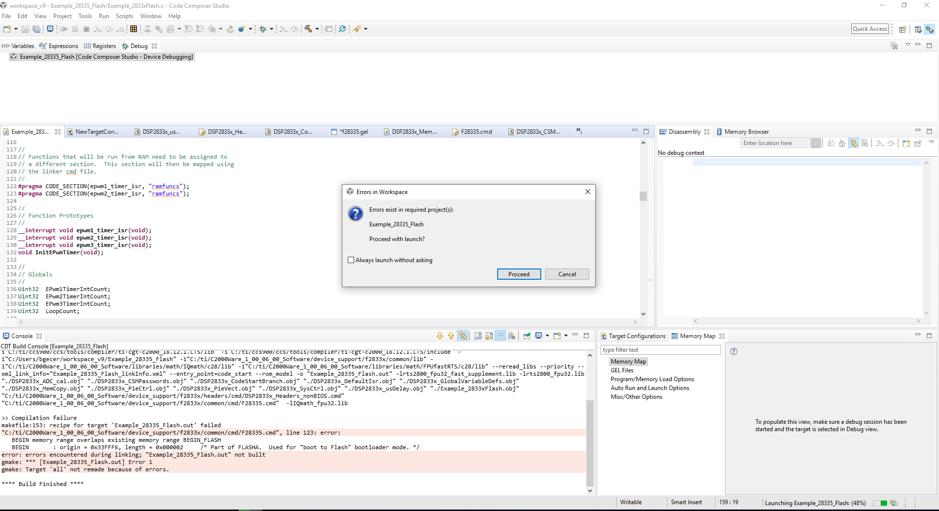
I can load program to TMS320F28335 DSP Controller on DSP Development Board using CCS 5. I can run code (led blink) perfectly and I can see led blinks. 

If I reset my board (cut off energy from development board),after reset, leds dont blink.

I cant run my application after reset DSP.

What Should I do?

I wait your return soon possible.

Thanks.


  • GC,

    Are you placing the program in RAM or FLASH?  If the program is being placed in RAM then it will be gone after removing power from your development board.

    Regards,

    John

  • Hi,

    Firstly, Thank for your reply,

    I have tried to place program in Flash and I have tried to executing my code from flash after a DSP Reset.(I followed TI documents in Addition.) But I couldnt solve problem.

    Could You share a tutorial or another document with me to solve this problem ?

    Thanks.spra958l.pdfspraal3.pdf

  • GC,

    Are you setting up the boot mode pins correctly to boot from Flash on release from reset?

    http://www.ti.com/document-viewer/TMS320F28335/datasheet/boot-rom-litsprs230-0453#litSPRS230-0453 

    Best,
    Matthew

  • Hi,

    Yes, I set mode F to boot from flash.

    Thanks.

  • GC,

    Let's try and use one of the pre-built examples that is built for flash run and:

    1)Make sure it runs correctly on your setup

    2)Assuming #1, look for differences in the linker/main.c from you code.

    Code is in TIREX/cloud here http://dev.ti.com/tirex/explore/node?compilers=ccs&node=AEs.g7dc7ZmMMK6BdE5vqQ__gYkahfz__LATEST

    If you are using standalone CCS with C2000Ware it is here: C:\ti\c2000\C2000Ware_2_00_00_02\device_support\f2833x\examples\flash_f28335 

    Best,

    Matthew

  • Hi,

    I followed this steps.But there is still a problem.The Gel file make error.

    1-Could You share configured gel file (according to running from flash and flash address is 0x33FFF6).

    2-What are the other configurations setting on files as ".asm", ".cmd" .

    Thanks.

  • I have followed "Running an Application from Internal Flash Memory on the TMS320F28xxx DSP" tutorial,a specially under "Executing Your Code from Flash after a DSP Reset" title. I have problems as below in screenshot  When I debug my code.

    Problem 1;

    Problem 2:After I proceed ,I get second error as below:

    Problem 3:After I ok on Problem 2, get error as below;

    What Should I do ?

    Thanks.

  • Hi again,

    I solved my problem about F28335.cmd. (I can create Flash.out file and I can run my application.) BUT When I reset my experiment Kit, I cant run application after reset again.I still have same problem.

    They are my DSP2833x_CodeStartBranch.asm, DSP2833x_Headers_nonBIOS.cmd and  F28335.cmd (Linker Command File For F28335 Device) files;

    1- DSP2833x_CodeStartBranch.asm

    ***********************************************************************

    WD_DISABLE .set 0 ;set to 1 to disable WD, else set to 0

    .ref _c_int00
    .global code_start

    ***********************************************************************
    * Function: codestart section
    *
    * Description: Branch to code starting point
    ***********************************************************************


    code_start:
    .if WD_DISABLE == 1
    LB wd_disable ;Branch to watchdog disable code
    .else
    LB _c_int00 ;Branch to start of boot.asm in RTS library
    .endif

    ;end codestart section


    ***********************************************************************
    * Function: wd_disable
    *
    * Description: Disables the watchdog timer
    ***********************************************************************
    .if WD_DISABLE == 1

    .text
    wd_disable:
    SETC OBJMODE ;Set OBJMODE for 28x object code
    EALLOW ;Enable EALLOW protected register access
    MOVZ DP, #7029h>>6 ;Set data page for WDCR register
    MOV @7029h, #0068h ;Set WDDIS bit in WDCR to disable WD
    EDIS ;Disable EALLOW protected register access
    LB _c_int00 ;Branch to start of boot.asm in RTS library

    .endif

    ;end wd_disable

    .end

    ;//===========================================================================
    ;// End of file.
    ;//===========================================================================

    .ref _c_int00
    .sect "codestart"
    LB _c_int00 ;branch to start of code
    .end ;end of file CodeStartBranch.asm

    ...............................................................................................................................................................

    2-DSP2833x_Headers_nonBIOS.cmd 

    MEMORY
    {
    PAGE 0: /* Program Memory */
    BEGIN_FLASH : origin = 0x3F7FF6, length = 0x000002
    PAGE 1: /* Data Memory */

    DEV_EMU : origin = 0x000880, length = 0x000180 /* device emulation registers */
    FLASH_REGS : origin = 0x000A80, length = 0x000060 /* FLASH registers */
    CSM : origin = 0x000AE0, length = 0x000010 /* code security module registers */

    ADC_MIRROR : origin = 0x000B00, length = 0x000010 /* ADC Results register mirror */

    XINTF : origin = 0x000B20, length = 0x000020 /* external interface registers */

    CPU_TIMER0 : origin = 0x000C00, length = 0x000008 /* CPU Timer0 registers */
    CPU_TIMER1 : origin = 0x000C08, length = 0x000008 /* CPU Timer0 registers (CPU Timer1 & Timer2 reserved TI use)*/
    CPU_TIMER2 : origin = 0x000C10, length = 0x000008 /* CPU Timer0 registers (CPU Timer1 & Timer2 reserved TI use)*/

    PIE_CTRL : origin = 0x000CE0, length = 0x000020 /* PIE control registers */
    PIE_VECT : origin = 0x000D00, length = 0x000100 /* PIE Vector Table */

    DMA : origin = 0x001000, length = 0x000200 /* DMA registers */

    MCBSPA : origin = 0x005000, length = 0x000040 /* McBSP-A registers */
    MCBSPB : origin = 0x005040, length = 0x000040 /* McBSP-B registers */

    ECANA : origin = 0x006000, length = 0x000040 /* eCAN-A control and status registers */
    ECANA_LAM : origin = 0x006040, length = 0x000040 /* eCAN-A local acceptance masks */
    ECANA_MOTS : origin = 0x006080, length = 0x000040 /* eCAN-A message object time stamps */
    ECANA_MOTO : origin = 0x0060C0, length = 0x000040 /* eCAN-A object time-out registers */
    ECANA_MBOX : origin = 0x006100, length = 0x000100 /* eCAN-A mailboxes */

    ECANB : origin = 0x006200, length = 0x000040 /* eCAN-B control and status registers */
    ECANB_LAM : origin = 0x006240, length = 0x000040 /* eCAN-B local acceptance masks */
    ECANB_MOTS : origin = 0x006280, length = 0x000040 /* eCAN-B message object time stamps */
    ECANB_MOTO : origin = 0x0062C0, length = 0x000040 /* eCAN-B object time-out registers */
    ECANB_MBOX : origin = 0x006300, length = 0x000100 /* eCAN-B mailboxes */

    EPWM1 : origin = 0x006800, length = 0x000022 /* Enhanced PWM 1 registers */
    EPWM2 : origin = 0x006840, length = 0x000022 /* Enhanced PWM 2 registers */
    EPWM3 : origin = 0x006880, length = 0x000022 /* Enhanced PWM 3 registers */
    EPWM4 : origin = 0x0068C0, length = 0x000022 /* Enhanced PWM 4 registers */
    EPWM5 : origin = 0x006900, length = 0x000022 /* Enhanced PWM 5 registers */
    EPWM6 : origin = 0x006940, length = 0x000022 /* Enhanced PWM 6 registers */

    ECAP1 : origin = 0x006A00, length = 0x000020 /* Enhanced Capture 1 registers */
    ECAP2 : origin = 0x006A20, length = 0x000020 /* Enhanced Capture 2 registers */
    ECAP3 : origin = 0x006A40, length = 0x000020 /* Enhanced Capture 3 registers */
    ECAP4 : origin = 0x006A60, length = 0x000020 /* Enhanced Capture 4 registers */
    ECAP5 : origin = 0x006A80, length = 0x000020 /* Enhanced Capture 5 registers */
    ECAP6 : origin = 0x006AA0, length = 0x000020 /* Enhanced Capture 6 registers */

    EQEP1 : origin = 0x006B00, length = 0x000040 /* Enhanced QEP 1 registers */
    EQEP2 : origin = 0x006B40, length = 0x000040 /* Enhanced QEP 2 registers */

    GPIOCTRL : origin = 0x006F80, length = 0x000040 /* GPIO control registers */
    GPIODAT : origin = 0x006FC0, length = 0x000020 /* GPIO data registers */
    GPIOINT : origin = 0x006FE0, length = 0x000020 /* GPIO interrupt/LPM registers */

    SYSTEM : origin = 0x007010, length = 0x000020 /* System control registers */
    SPIA : origin = 0x007040, length = 0x000010 /* SPI-A registers */
    SCIA : origin = 0x007050, length = 0x000010 /* SCI-A registers */
    XINTRUPT : origin = 0x007070, length = 0x000010 /* external interrupt registers */

    ADC : origin = 0x007100, length = 0x000020 /* ADC registers */

    SCIB : origin = 0x007750, length = 0x000010 /* SCI-B registers */

    SCIC : origin = 0x007770, length = 0x000010 /* SCI-C registers */

    I2CA : origin = 0x007900, length = 0x000040 /* I2C-A registers */

    CSM_PWL : origin = 0x33FFF8, length = 0x000008 /* Part of FLASHA. CSM password locations. */

    PARTID : origin = 0x380090, length = 0x000001 /* Part ID register location */
    }


    SECTIONS
    {

    codestart: > BEGIN_FLASH, PAGE = 0

    PieVectTableFile : > PIE_VECT, PAGE = 1

    /*** Peripheral Frame 0 Register Structures ***/
    DevEmuRegsFile : > DEV_EMU, PAGE = 1
    FlashRegsFile : > FLASH_REGS, PAGE = 1
    CsmRegsFile : > CSM, PAGE = 1
    AdcMirrorFile : > ADC_MIRROR, PAGE = 1
    XintfRegsFile : > XINTF, PAGE = 1
    CpuTimer0RegsFile : > CPU_TIMER0, PAGE = 1
    CpuTimer1RegsFile : > CPU_TIMER1, PAGE = 1
    CpuTimer2RegsFile : > CPU_TIMER2, PAGE = 1
    PieCtrlRegsFile : > PIE_CTRL, PAGE = 1
    DmaRegsFile : > DMA, PAGE = 1

    /*** Peripheral Frame 3 Register Structures ***/
    McbspaRegsFile : > MCBSPA, PAGE = 1
    McbspbRegsFile : > MCBSPB, PAGE = 1

    /*** Peripheral Frame 1 Register Structures ***/
    ECanaRegsFile : > ECANA, PAGE = 1
    ECanaLAMRegsFile : > ECANA_LAM PAGE = 1
    ECanaMboxesFile : > ECANA_MBOX PAGE = 1
    ECanaMOTSRegsFile : > ECANA_MOTS PAGE = 1
    ECanaMOTORegsFile : > ECANA_MOTO PAGE = 1

    ECanbRegsFile : > ECANB, PAGE = 1
    ECanbLAMRegsFile : > ECANB_LAM PAGE = 1
    ECanbMboxesFile : > ECANB_MBOX PAGE = 1
    ECanbMOTSRegsFile : > ECANB_MOTS PAGE = 1
    ECanbMOTORegsFile : > ECANB_MOTO PAGE = 1

    EPwm1RegsFile : > EPWM1 PAGE = 1
    EPwm2RegsFile : > EPWM2 PAGE = 1
    EPwm3RegsFile : > EPWM3 PAGE = 1
    EPwm4RegsFile : > EPWM4 PAGE = 1
    EPwm5RegsFile : > EPWM5 PAGE = 1
    EPwm6RegsFile : > EPWM6 PAGE = 1

    ECap1RegsFile : > ECAP1 PAGE = 1
    ECap2RegsFile : > ECAP2 PAGE = 1
    ECap3RegsFile : > ECAP3 PAGE = 1
    ECap4RegsFile : > ECAP4 PAGE = 1
    ECap5RegsFile : > ECAP5 PAGE = 1
    ECap6RegsFile : > ECAP6 PAGE = 1

    EQep1RegsFile : > EQEP1 PAGE = 1
    EQep2RegsFile : > EQEP2 PAGE = 1

    GpioCtrlRegsFile : > GPIOCTRL PAGE = 1
    GpioDataRegsFile : > GPIODAT PAGE = 1
    GpioIntRegsFile : > GPIOINT PAGE = 1

    /*** Peripheral Frame 2 Register Structures ***/
    SysCtrlRegsFile : > SYSTEM, PAGE = 1
    SpiaRegsFile : > SPIA, PAGE = 1
    SciaRegsFile : > SCIA, PAGE = 1
    XIntruptRegsFile : > XINTRUPT, PAGE = 1
    AdcRegsFile : > ADC, PAGE = 1
    ScibRegsFile : > SCIB, PAGE = 1
    ScicRegsFile : > SCIC, PAGE = 1
    I2caRegsFile : > I2CA, PAGE = 1

    /*** Code Security Module Register Structures ***/
    CsmPwlFile : > CSM_PWL, PAGE = 1

    /*** Device Part ID Register Structures ***/
    PartIdRegsFile : > PARTID, PAGE = 1

    }


    /*
    //===========================================================================
    // End of file.
    //===========================================================================
    */

    ........................................................................................................................................................................

    3-      // FILE: F28335.cmd

    // TITLE: Linker Command File For F28335 Device

    MEMORY
    {
    PAGE 0: /* Program Memory */
    /* Memory (RAM/FLASH/OTP) blocks can be moved to PAGE1 for data allocation */

    ZONE0 : origin = 0x004000, length = 0x001000 /* XINTF zone 0 */
    RAML0 : origin = 0x008000, length = 0x001000 /* on-chip RAM block L0 */
    RAML1 : origin = 0x009000, length = 0x001000 /* on-chip RAM block L1 */
    RAML2 : origin = 0x00A000, length = 0x001000 /* on-chip RAM block L2 */
    RAML3 : origin = 0x00B000, length = 0x001000 /* on-chip RAM block L3 */
    ZONE6 : origin = 0x0100000, length = 0x100000 /* XINTF zone 6 */
    ZONE7A : origin = 0x0200000, length = 0x00FC00 /* XINTF zone 7 - program space */
    FLASHH : origin = 0x300000, length = 0x008000 /* on-chip FLASH */
    FLASHG : origin = 0x308000, length = 0x008000 /* on-chip FLASH */
    FLASHF : origin = 0x310000, length = 0x008000 /* on-chip FLASH */
    FLASHE : origin = 0x318000, length = 0x008000 /* on-chip FLASH */
    FLASHD : origin = 0x320000, length = 0x008000 /* on-chip FLASH */
    FLASHC : origin = 0x328000, length = 0x008000 /* on-chip FLASH */
    FLASHA : origin = 0x338000, length = 0x007F80 /* on-chip FLASH */
    CSM_RSVD : origin = 0x33FF80, length = 0x000076 /* Part of FLASHA. Program with all 0x0000 when CSM is in use. */
    BEGIN : origin = 0x33FFF6, length = 0x000002 /* Part of FLASHA. Used for "boot to Flash" bootloader mode. */
    CSM_PWL : origin = 0x33FFF8, length = 0x000008 /* Part of FLASHA. CSM password locations in FLASHA */
    OTP : origin = 0x380400, length = 0x000400 /* on-chip OTP */
    ADC_CAL : origin = 0x380080, length = 0x000009 /* ADC_cal function in Reserved memory */

    IQTABLES : origin = 0x3FE000, length = 0x000b50 /* IQ Math Tables in Boot ROM */
    IQTABLES2 : origin = 0x3FEB50, length = 0x00008c /* IQ Math Tables in Boot ROM */
    FPUTABLES : origin = 0x3FEBDC, length = 0x0006A0 /* FPU Tables in Boot ROM */
    ROM : origin = 0x3FF27C, length = 0x000D44 /* Boot ROM */
    RESET : origin = 0x3FFFC0, length = 0x000002 /* part of boot ROM */
    VECTORS : origin = 0x3FFFC2, length = 0x00003E /* part of boot ROM */

    PAGE 1 : /* Data Memory */
    /* Memory (RAM/FLASH/OTP) blocks can be moved to PAGE0 for program allocation */
    /* Registers remain on PAGE1 */

    BOOT_RSVD : origin = 0x000000, length = 0x000050 /* Part of M0, BOOT rom will use this for stack */
    RAMM0 : origin = 0x000050, length = 0x0003B0 /* on-chip RAM block M0 */
    RAMM1 : origin = 0x000400, length = 0x000400 /* on-chip RAM block M1 */
    RAML4 : origin = 0x00C000, length = 0x001000 /* on-chip RAM block L1 */
    RAML5 : origin = 0x00D000, length = 0x001000 /* on-chip RAM block L1 */
    RAML6 : origin = 0x00E000, length = 0x001000 /* on-chip RAM block L1 */
    RAML7 : origin = 0x00F000, length = 0x001000 /* on-chip RAM block L1 */
    ZONE7B : origin = 0x20FC00, length = 0x000400 /* XINTF zone 7 - data space */
    FLASHB : origin = 0x330000, length = 0x008000 /* on-chip FLASH */
    }

    /* Allocate sections to memory blocks.
    Note:
    codestart user defined section in DSP28_CodeStartBranch.asm used to redirect code
    execution when booting to flash
    ramfuncs user defined section to store functions that will be copied from Flash into RAM
    */

    SECTIONS
    {

    /* Allocate program areas: */
    .cinit : > FLASHA PAGE = 0
    .pinit : > FLASHA, PAGE = 0
    .text : > FLASHA PAGE = 0
    codestart : > BEGIN_FLASH, PAGE = 0
    ramfuncs : LOAD = FLASHD,
    RUN = RAML0,
    LOAD_START(_RamfuncsLoadStart),
    LOAD_END(_RamfuncsLoadEnd),
    RUN_START(_RamfuncsRunStart),
    LOAD_SIZE(_RamfuncsLoadSize),
    PAGE = 0

    csmpasswds : > CSM_PWL PAGE = 0
    csm_rsvd : > CSM_RSVD PAGE = 0

    /* Allocate uninitalized data sections: */
    .stack : > RAMM1 PAGE = 1
    .ebss : > RAML4 PAGE = 1
    .esysmem : > RAMM1 PAGE = 1

    /* Initalized sections go in Flash */
    /* For SDFlash to program these, they must be allocated to page 0 */
    .econst : > FLASHA PAGE = 0
    .switch : > FLASHA PAGE = 0

    /* Allocate IQ math areas: */
    IQmath : > FLASHC PAGE = 0 /* Math Code */
    IQmathTables : > IQTABLES, PAGE = 0, TYPE = NOLOAD

    /* Uncomment the section below if calling the IQNexp() or IQexp()
    functions from the IQMath.lib library in order to utilize the
    relevant IQ Math table in Boot ROM (This saves space and Boot ROM
    is 1 wait-state). If this section is not uncommented, IQmathTables2
    will be loaded into other memory (SARAM, Flash, etc.) and will take
    up space, but 0 wait-state is possible.
    */
    /*
    IQmathTables2 : > IQTABLES2, PAGE = 0, TYPE = NOLOAD
    {

    IQmath.lib<IQNexpTable.obj> (IQmathTablesRam)

    }
    */

    FPUmathTables : > FPUTABLES, PAGE = 0, TYPE = NOLOAD

    /* Allocate DMA-accessible RAM sections: */
    DMARAML4 : > RAML4, PAGE = 1
    DMARAML5 : > RAML5, PAGE = 1
    DMARAML6 : > RAML6, PAGE = 1
    DMARAML7 : > RAML7, PAGE = 1

    /* Allocate 0x400 of XINTF Zone 7 to storing data */
    ZONE7DATA : > ZONE7B, PAGE = 1

    /* .reset is a standard section used by the compiler. It contains the */
    /* the address of the start of _c_int00 for C Code. /*
    /* When using the boot ROM this section and the CPU vector */
    /* table is not needed. Thus the default type is set here to */
    /* DSECT */
    .reset : > RESET, PAGE = 0, TYPE = DSECT
    vectors : > VECTORS PAGE = 0, TYPE = DSECT

    /* Allocate ADC_cal function (pre-programmed by factory into TI reserved memory) */
    .adc_cal : load = ADC_CAL, PAGE = 0, TYPE = NOLOAD

    }

    /*
    //===========================================================================
    // End of file.
    //===========================================================================
    */

    .....................................................................................................................................................................................................................

    ARE ALL FILES OKAY ?


    What Shoul I do? 


    Thanks .


  • I'm adding some more TI side people to the thread to look at the code you attached and why the example is failing to build, it looks like there are some overloaded defines.

    The GEL error is just because the load had an issue, I don't think a new GEL file is needed here.  The newer version of CCS should be programming the flash as you load, do you observe some dialogue boxes when you load the program, showing erasing/programming/ etc?  If not we may need to manually program the code with the flash tools.

    Best,
    Matthew

  • Hi,  

    Firstly, Thanks for your response,

    I use CCS 9.0.But I also tried CCS 5 and CCS 6 too. 

    Yes, I observe erasing,programming etc. When I load program.

    Thanks.

  • hi ,

    1. The linker issue seem to be because of having 2 memory sections mapped to the same memory region.

    MEMORY
    {
    PAGE 0: /* Program Memory */
    BEGIN_FLASH : origin = 0x3F7FF6, length = 0x000002

    why do you have a BEGIN_FLASH in DSP2833x_Headers_nonBIOS.cmd file , doesn't the F28335.cmd already have BEGIN ?

    BEGIN : origin = 0x33FFF6, length = 0x000002 /* Part of FLASHA. Used for "boot to Flash" bootloader mode. */

    2. Please remove references of BEGIN from DSP2833x_Headers_nonBIOS.cmd the and keep it only in the F28335.cmd file.


    The DSP2833x_Headers_nonBIOS.cmd is primarily to map the peripherals to there memory spaces .


    All other memory usages including codestart can remain in the F28335.cmd file.

    Move back the codestart to point to the BEGIN in the default cmd file and remove any usage of BEGIN_FLASH from both cmd files.


    codestart : > BEGIN_FLASH, PAGE = 0

    Regards.

  • Hi,

    Thanks for your response,

    I edited them according your commends:

    Are they okay now?

    1- FILE: DSP2833x_Headers_nonBIOS.cmd

    // TI File $Revision: /main/8 $
    // Checkin $Date: June 2, 2008 11:12:24 $
    //###########################################################################
    //
    // FILE: DSP2833x_Headers_nonBIOS.cmd
    //
    // TITLE: DSP2833x Peripheral registers linker command file
    //
    // DESCRIPTION:
    //
    // This file is for use in Non-BIOS applications.
    //
    // Linker command file to place the peripheral structures
    // used within the DSP2833x headerfiles into the correct memory
    // mapped locations.
    //
    // This version of the file includes the PieVectorTable structure.
    // For BIOS applications, please use the DSP2833x_Headers_BIOS.cmd file
    // which does not include the PieVectorTable structure.
    //
    //###########################################################################
    // $TI Release: F2833x Support Library v2.00.00.00 $
    // $Release Date: Thu Oct 18 15:47:35 CDT 2018 $
    // $Copyright:
    // Copyright (C) 2009-2018 Texas Instruments Incorporated - http://www.ti.com/
    //
    // Redistribution and use in source and binary forms, with or without
    // modification, are permitted provided that the following conditions
    // are met:
    //
    // Redistributions of source code must retain the above copyright
    // notice, this list of conditions and the following disclaimer.
    //
    // Redistributions in binary form must reproduce the above copyright
    // notice, this list of conditions and the following disclaimer in the
    // documentation and/or other materials provided with the
    // distribution.
    //
    // Neither the name of Texas Instruments Incorporated nor the names of
    // its contributors may be used to endorse or promote products derived
    // from this software without specific prior written permission.
    //
    // THIS SOFTWARE IS PROVIDED BY THE COPYRIGHT HOLDERS AND CONTRIBUTORS
    // "AS IS" AND ANY EXPRESS OR IMPLIED WARRANTIES, INCLUDING, BUT NOT
    // LIMITED TO, THE IMPLIED WARRANTIES OF MERCHANTABILITY AND FITNESS FOR
    // A PARTICULAR PURPOSE ARE DISCLAIMED. IN NO EVENT SHALL THE COPYRIGHT
    // OWNER OR CONTRIBUTORS BE LIABLE FOR ANY DIRECT, INDIRECT, INCIDENTAL,
    // SPECIAL, EXEMPLARY, OR CONSEQUENTIAL DAMAGES (INCLUDING, BUT NOT
    // LIMITED TO, PROCUREMENT OF SUBSTITUTE GOODS OR SERVICES; LOSS OF USE,
    // DATA, OR PROFITS; OR BUSINESS INTERRUPTION) HOWEVER CAUSED AND ON ANY
    // THEORY OF LIABILITY, WHETHER IN CONTRACT, STRICT LIABILITY, OR TORT
    // (INCLUDING NEGLIGENCE OR OTHERWISE) ARISING IN ANY WAY OUT OF THE USE
    // OF THIS SOFTWARE, EVEN IF ADVISED OF THE POSSIBILITY OF SUCH DAMAGE.
    // $
    //###########################################################################
    */

    MEMORY
    {
    PAGE 0: /* Program Memory */
    //BEGIN_FLASH : origin = 0x3F7FF6, length = 0x000002
    PAGE 1: /* Data Memory */

    DEV_EMU : origin = 0x000880, length = 0x000180 /* device emulation registers */
    FLASH_REGS : origin = 0x000A80, length = 0x000060 /* FLASH registers */
    CSM : origin = 0x000AE0, length = 0x000010 /* code security module registers */

    ADC_MIRROR : origin = 0x000B00, length = 0x000010 /* ADC Results register mirror */

    XINTF : origin = 0x000B20, length = 0x000020 /* external interface registers */

    CPU_TIMER0 : origin = 0x000C00, length = 0x000008 /* CPU Timer0 registers */
    CPU_TIMER1 : origin = 0x000C08, length = 0x000008 /* CPU Timer0 registers (CPU Timer1 & Timer2 reserved TI use)*/
    CPU_TIMER2 : origin = 0x000C10, length = 0x000008 /* CPU Timer0 registers (CPU Timer1 & Timer2 reserved TI use)*/

    PIE_CTRL : origin = 0x000CE0, length = 0x000020 /* PIE control registers */
    PIE_VECT : origin = 0x000D00, length = 0x000100 /* PIE Vector Table */

    DMA : origin = 0x001000, length = 0x000200 /* DMA registers */

    MCBSPA : origin = 0x005000, length = 0x000040 /* McBSP-A registers */
    MCBSPB : origin = 0x005040, length = 0x000040 /* McBSP-B registers */

    ECANA : origin = 0x006000, length = 0x000040 /* eCAN-A control and status registers */
    ECANA_LAM : origin = 0x006040, length = 0x000040 /* eCAN-A local acceptance masks */
    ECANA_MOTS : origin = 0x006080, length = 0x000040 /* eCAN-A message object time stamps */
    ECANA_MOTO : origin = 0x0060C0, length = 0x000040 /* eCAN-A object time-out registers */
    ECANA_MBOX : origin = 0x006100, length = 0x000100 /* eCAN-A mailboxes */

    ECANB : origin = 0x006200, length = 0x000040 /* eCAN-B control and status registers */
    ECANB_LAM : origin = 0x006240, length = 0x000040 /* eCAN-B local acceptance masks */
    ECANB_MOTS : origin = 0x006280, length = 0x000040 /* eCAN-B message object time stamps */
    ECANB_MOTO : origin = 0x0062C0, length = 0x000040 /* eCAN-B object time-out registers */
    ECANB_MBOX : origin = 0x006300, length = 0x000100 /* eCAN-B mailboxes */

    EPWM1 : origin = 0x006800, length = 0x000022 /* Enhanced PWM 1 registers */
    EPWM2 : origin = 0x006840, length = 0x000022 /* Enhanced PWM 2 registers */
    EPWM3 : origin = 0x006880, length = 0x000022 /* Enhanced PWM 3 registers */
    EPWM4 : origin = 0x0068C0, length = 0x000022 /* Enhanced PWM 4 registers */
    EPWM5 : origin = 0x006900, length = 0x000022 /* Enhanced PWM 5 registers */
    EPWM6 : origin = 0x006940, length = 0x000022 /* Enhanced PWM 6 registers */

    ECAP1 : origin = 0x006A00, length = 0x000020 /* Enhanced Capture 1 registers */
    ECAP2 : origin = 0x006A20, length = 0x000020 /* Enhanced Capture 2 registers */
    ECAP3 : origin = 0x006A40, length = 0x000020 /* Enhanced Capture 3 registers */
    ECAP4 : origin = 0x006A60, length = 0x000020 /* Enhanced Capture 4 registers */
    ECAP5 : origin = 0x006A80, length = 0x000020 /* Enhanced Capture 5 registers */
    ECAP6 : origin = 0x006AA0, length = 0x000020 /* Enhanced Capture 6 registers */

    EQEP1 : origin = 0x006B00, length = 0x000040 /* Enhanced QEP 1 registers */
    EQEP2 : origin = 0x006B40, length = 0x000040 /* Enhanced QEP 2 registers */

    GPIOCTRL : origin = 0x006F80, length = 0x000040 /* GPIO control registers */
    GPIODAT : origin = 0x006FC0, length = 0x000020 /* GPIO data registers */
    GPIOINT : origin = 0x006FE0, length = 0x000020 /* GPIO interrupt/LPM registers */

    SYSTEM : origin = 0x007010, length = 0x000020 /* System control registers */
    SPIA : origin = 0x007040, length = 0x000010 /* SPI-A registers */
    SCIA : origin = 0x007050, length = 0x000010 /* SCI-A registers */
    XINTRUPT : origin = 0x007070, length = 0x000010 /* external interrupt registers */

    ADC : origin = 0x007100, length = 0x000020 /* ADC registers */

    SCIB : origin = 0x007750, length = 0x000010 /* SCI-B registers */

    SCIC : origin = 0x007770, length = 0x000010 /* SCI-C registers */

    I2CA : origin = 0x007900, length = 0x000040 /* I2C-A registers */

    CSM_PWL : origin = 0x33FFF8, length = 0x000008 /* Part of FLASHA. CSM password locations. */

    PARTID : origin = 0x380090, length = 0x000001 /* Part ID register location */
    }


    SECTIONS
    {

    //codestart: > BEGIN_FLASH, PAGE = 0

    PieVectTableFile : > PIE_VECT, PAGE = 1

    /*** Peripheral Frame 0 Register Structures ***/
    DevEmuRegsFile : > DEV_EMU, PAGE = 1
    FlashRegsFile : > FLASH_REGS, PAGE = 1
    CsmRegsFile : > CSM, PAGE = 1
    AdcMirrorFile : > ADC_MIRROR, PAGE = 1
    XintfRegsFile : > XINTF, PAGE = 1
    CpuTimer0RegsFile : > CPU_TIMER0, PAGE = 1
    CpuTimer1RegsFile : > CPU_TIMER1, PAGE = 1
    CpuTimer2RegsFile : > CPU_TIMER2, PAGE = 1
    PieCtrlRegsFile : > PIE_CTRL, PAGE = 1
    DmaRegsFile : > DMA, PAGE = 1

    /*** Peripheral Frame 3 Register Structures ***/
    McbspaRegsFile : > MCBSPA, PAGE = 1
    McbspbRegsFile : > MCBSPB, PAGE = 1

    /*** Peripheral Frame 1 Register Structures ***/
    ECanaRegsFile : > ECANA, PAGE = 1
    ECanaLAMRegsFile : > ECANA_LAM PAGE = 1
    ECanaMboxesFile : > ECANA_MBOX PAGE = 1
    ECanaMOTSRegsFile : > ECANA_MOTS PAGE = 1
    ECanaMOTORegsFile : > ECANA_MOTO PAGE = 1

    ECanbRegsFile : > ECANB, PAGE = 1
    ECanbLAMRegsFile : > ECANB_LAM PAGE = 1
    ECanbMboxesFile : > ECANB_MBOX PAGE = 1
    ECanbMOTSRegsFile : > ECANB_MOTS PAGE = 1
    ECanbMOTORegsFile : > ECANB_MOTO PAGE = 1

    EPwm1RegsFile : > EPWM1 PAGE = 1
    EPwm2RegsFile : > EPWM2 PAGE = 1
    EPwm3RegsFile : > EPWM3 PAGE = 1
    EPwm4RegsFile : > EPWM4 PAGE = 1
    EPwm5RegsFile : > EPWM5 PAGE = 1
    EPwm6RegsFile : > EPWM6 PAGE = 1

    ECap1RegsFile : > ECAP1 PAGE = 1
    ECap2RegsFile : > ECAP2 PAGE = 1
    ECap3RegsFile : > ECAP3 PAGE = 1
    ECap4RegsFile : > ECAP4 PAGE = 1
    ECap5RegsFile : > ECAP5 PAGE = 1
    ECap6RegsFile : > ECAP6 PAGE = 1

    EQep1RegsFile : > EQEP1 PAGE = 1
    EQep2RegsFile : > EQEP2 PAGE = 1

    GpioCtrlRegsFile : > GPIOCTRL PAGE = 1
    GpioDataRegsFile : > GPIODAT PAGE = 1
    GpioIntRegsFile : > GPIOINT PAGE = 1

    /*** Peripheral Frame 2 Register Structures ***/
    SysCtrlRegsFile : > SYSTEM, PAGE = 1
    SpiaRegsFile : > SPIA, PAGE = 1
    SciaRegsFile : > SCIA, PAGE = 1
    XIntruptRegsFile : > XINTRUPT, PAGE = 1
    AdcRegsFile : > ADC, PAGE = 1
    ScibRegsFile : > SCIB, PAGE = 1
    ScicRegsFile : > SCIC, PAGE = 1
    I2caRegsFile : > I2CA, PAGE = 1

    /*** Code Security Module Register Structures ***/
    CsmPwlFile : > CSM_PWL, PAGE = 1

    /*** Device Part ID Register Structures ***/
    PartIdRegsFile : > PARTID, PAGE = 1

    }


    /*
    //===========================================================================
    // End of file.
    //===========================================================================
    */

    2- // FILE: F28335.cmd

    /*
    //###########################################################################
    //
    // FILE: F28335.cmd
    //
    // TITLE: Linker Command File For F28335 Device
    //
    //###########################################################################
    // $TI Release: F2833x/F2823x Header Files and Peripheral Examples V140 $
    // $Release Date: March 4, 2015 $
    // $Copyright: Copyright (C) 2007-2015 Texas Instruments Incorporated -
    // http://www.ti.com/ ALL RIGHTS RESERVED $
    //###########################################################################
    */

    /* ======================================================
    // For Code Composer Studio V2.2 and later
    // ---------------------------------------
    // In addition to this memory linker command file,
    // add the header linker command file directly to the project.
    // The header linker command file is required to link the
    // peripheral structures to the proper locations within
    // the memory map.
    //
    // The header linker files are found in <base>\DSP2833x_Headers\cmd
    //
    // For BIOS applications add: DSP2833x_Headers_BIOS.cmd
    // For nonBIOS applications add: DSP2833x_Headers_nonBIOS.cmd
    ========================================================= */

    /* ======================================================
    // For Code Composer Studio prior to V2.2
    // --------------------------------------
    // 1) Use one of the following -l statements to include the
    // header linker command file in the project. The header linker
    // file is required to link the peripheral structures to the proper
    // locations within the memory map */

    /* Uncomment this line to include file only for non-BIOS applications */
    /* -l DSP2833x_Headers_nonBIOS.cmd */

    /* Uncomment this line to include file only for BIOS applications */
    /* -l DSP2833x_Headers_BIOS.cmd */

    /* 2) In your project add the path to <base>\DSP2833x_headers\cmd to the
    library search path under project->build options, linker tab,
    library search path (-i).
    /*========================================================= */

    /* Define the memory block start/length for the F28335
    PAGE 0 will be used to organize program sections
    PAGE 1 will be used to organize data sections

    Notes:
    Memory blocks on F28335 are uniform (ie same
    physical memory) in both PAGE 0 and PAGE 1.
    That is the same memory region should not be
    defined for both PAGE 0 and PAGE 1.
    Doing so will result in corruption of program
    and/or data.

    L0/L1/L2 and L3 memory blocks are mirrored - that is
    they can be accessed in high memory or low memory.
    For simplicity only one instance is used in this
    linker file.

    Contiguous SARAM memory blocks can be combined
    if required to create a larger memory block.
    */


    MEMORY
    {
    PAGE 0: /* Program Memory */
    /* Memory (RAM/FLASH/OTP) blocks can be moved to PAGE1 for data allocation */

    ZONE0 : origin = 0x004000, length = 0x001000 /* XINTF zone 0 */
    RAML0 : origin = 0x008000, length = 0x001000 /* on-chip RAM block L0 */
    RAML1 : origin = 0x009000, length = 0x001000 /* on-chip RAM block L1 */
    RAML2 : origin = 0x00A000, length = 0x001000 /* on-chip RAM block L2 */
    RAML3 : origin = 0x00B000, length = 0x001000 /* on-chip RAM block L3 */
    ZONE6 : origin = 0x0100000, length = 0x100000 /* XINTF zone 6 */
    ZONE7A : origin = 0x0200000, length = 0x00FC00 /* XINTF zone 7 - program space */
    FLASHH : origin = 0x300000, length = 0x008000 /* on-chip FLASH */
    FLASHG : origin = 0x308000, length = 0x008000 /* on-chip FLASH */
    FLASHF : origin = 0x310000, length = 0x008000 /* on-chip FLASH */
    FLASHE : origin = 0x318000, length = 0x008000 /* on-chip FLASH */
    FLASHD : origin = 0x320000, length = 0x008000 /* on-chip FLASH */
    FLASHC : origin = 0x328000, length = 0x008000 /* on-chip FLASH */
    FLASHA : origin = 0x338000, length = 0x007F80 /* on-chip FLASH */
    CSM_RSVD : origin = 0x33FF80, length = 0x000076 /* Part of FLASHA. Program with all 0x0000 when CSM is in use. */
    BEGIN : origin = 0x33FFF6, length = 0x000002 /* Part of FLASHA. Used for "boot to Flash" bootloader mode. */
    CSM_PWL : origin = 0x33FFF8, length = 0x000008 /* Part of FLASHA. CSM password locations in FLASHA */
    OTP : origin = 0x380400, length = 0x000400 /* on-chip OTP */
    ADC_CAL : origin = 0x380080, length = 0x000009 /* ADC_cal function in Reserved memory */

    IQTABLES : origin = 0x3FE000, length = 0x000b50 /* IQ Math Tables in Boot ROM */
    IQTABLES2 : origin = 0x3FEB50, length = 0x00008c /* IQ Math Tables in Boot ROM */
    FPUTABLES : origin = 0x3FEBDC, length = 0x0006A0 /* FPU Tables in Boot ROM */
    ROM : origin = 0x3FF27C, length = 0x000D44 /* Boot ROM */
    RESET : origin = 0x3FFFC0, length = 0x000002 /* part of boot ROM */
    VECTORS : origin = 0x3FFFC2, length = 0x00003E /* part of boot ROM */

    PAGE 1 : /* Data Memory */
    /* Memory (RAM/FLASH/OTP) blocks can be moved to PAGE0 for program allocation */
    /* Registers remain on PAGE1 */

    BOOT_RSVD : origin = 0x000000, length = 0x000050 /* Part of M0, BOOT rom will use this for stack */
    RAMM0 : origin = 0x000050, length = 0x0003B0 /* on-chip RAM block M0 */
    RAMM1 : origin = 0x000400, length = 0x000400 /* on-chip RAM block M1 */
    RAML4 : origin = 0x00C000, length = 0x001000 /* on-chip RAM block L1 */
    RAML5 : origin = 0x00D000, length = 0x001000 /* on-chip RAM block L1 */
    RAML6 : origin = 0x00E000, length = 0x001000 /* on-chip RAM block L1 */
    RAML7 : origin = 0x00F000, length = 0x001000 /* on-chip RAM block L1 */
    ZONE7B : origin = 0x20FC00, length = 0x000400 /* XINTF zone 7 - data space */
    FLASHB : origin = 0x330000, length = 0x008000 /* on-chip FLASH */
    }

    /* Allocate sections to memory blocks.
    Note:
    codestart user defined section in DSP28_CodeStartBranch.asm used to redirect code
    execution when booting to flash
    ramfuncs user defined section to store functions that will be copied from Flash into RAM
    */

    SECTIONS
    {

    /* Allocate program areas: */
    .cinit : > FLASHA PAGE = 0
    .pinit : > FLASHA, PAGE = 0
    .text : > FLASHA PAGE = 0
    // codestart : > BEGIN_FLASH, PAGE = 0
    ramfuncs : LOAD = FLASHD,
    RUN = RAML0,
    LOAD_START(_RamfuncsLoadStart),
    LOAD_END(_RamfuncsLoadEnd),
    RUN_START(_RamfuncsRunStart),
    LOAD_SIZE(_RamfuncsLoadSize),
    PAGE = 0

    csmpasswds : > CSM_PWL PAGE = 0
    csm_rsvd : > CSM_RSVD PAGE = 0

    /* Allocate uninitalized data sections: */
    .stack : > RAMM1 PAGE = 1
    .ebss : > RAML4 PAGE = 1
    .esysmem : > RAMM1 PAGE = 1

    /* Initalized sections go in Flash */
    /* For SDFlash to program these, they must be allocated to page 0 */
    .econst : > FLASHA PAGE = 0
    .switch : > FLASHA PAGE = 0

    /* Allocate IQ math areas: */
    IQmath : > FLASHC PAGE = 0 /* Math Code */
    IQmathTables : > IQTABLES, PAGE = 0, TYPE = NOLOAD

    /* Uncomment the section below if calling the IQNexp() or IQexp()
    functions from the IQMath.lib library in order to utilize the
    relevant IQ Math table in Boot ROM (This saves space and Boot ROM
    is 1 wait-state). If this section is not uncommented, IQmathTables2
    will be loaded into other memory (SARAM, Flash, etc.) and will take
    up space, but 0 wait-state is possible.
    */
    /*
    IQmathTables2 : > IQTABLES2, PAGE = 0, TYPE = NOLOAD
    {

    IQmath.lib<IQNexpTable.obj> (IQmathTablesRam)

    }
    */

    FPUmathTables : > FPUTABLES, PAGE = 0, TYPE = NOLOAD

    /* Allocate DMA-accessible RAM sections: */
    DMARAML4 : > RAML4, PAGE = 1
    DMARAML5 : > RAML5, PAGE = 1
    DMARAML6 : > RAML6, PAGE = 1
    DMARAML7 : > RAML7, PAGE = 1

    /* Allocate 0x400 of XINTF Zone 7 to storing data */
    ZONE7DATA : > ZONE7B, PAGE = 1

    /* .reset is a standard section used by the compiler. It contains the */
    /* the address of the start of _c_int00 for C Code. /*
    /* When using the boot ROM this section and the CPU vector */
    /* table is not needed. Thus the default type is set here to */
    /* DSECT */
    .reset : > RESET, PAGE = 0, TYPE = DSECT
    vectors : > VECTORS PAGE = 0, TYPE = DSECT

    /* Allocate ADC_cal function (pre-programmed by factory into TI reserved memory) */
    .adc_cal : load = ADC_CAL, PAGE = 0, TYPE = NOLOAD

    }

    /*
    //===========================================================================
    // End of file.
    //===========================================================================
    */

    If there is a mistake, Could you edit it please and send to me ?

    Thank you for your help.

  • hi ,

    Uncomment this line in F28335.cmd to use BEGIN instead of BEGIN_FLASH.

    // codestart : > BEGIN_FLASH, PAGE = 0

    to 

    codestart : > BEGIN, PAGE = 0

    Rest looks fine. Please compile , load and check if you still see issues.

    Regards.

  • Hi,

    I changed  F28335.cmd file according to your advive as below,compiled and load program.My application run but after reset It didnt run. I still have same problem.

    // FILE: F28335.cmd

    /*
    //###########################################################################
    //
    // FILE: F28335.cmd
    //
    // TITLE: Linker Command File For F28335 Device
    //
    //###########################################################################
    // $TI Release: F2833x/F2823x Header Files and Peripheral Examples V140 $
    // $Release Date: March 4, 2015 $
    // $Copyright: Copyright (C) 2007-2015 Texas Instruments Incorporated -
    // http://www.ti.com/ ALL RIGHTS RESERVED $
    //###########################################################################
    */

    /* ======================================================
    // For Code Composer Studio V2.2 and later
    // ---------------------------------------
    // In addition to this memory linker command file,
    // add the header linker command file directly to the project.
    // The header linker command file is required to link the
    // peripheral structures to the proper locations within
    // the memory map.
    //
    // The header linker files are found in <base>\DSP2833x_Headers\cmd
    //
    // For BIOS applications add: DSP2833x_Headers_BIOS.cmd
    // For nonBIOS applications add: DSP2833x_Headers_nonBIOS.cmd
    ========================================================= */

    /* ======================================================
    // For Code Composer Studio prior to V2.2
    // --------------------------------------
    // 1) Use one of the following -l statements to include the
    // header linker command file in the project. The header linker
    // file is required to link the peripheral structures to the proper
    // locations within the memory map */

    /* Uncomment this line to include file only for non-BIOS applications */
    /* -l DSP2833x_Headers_nonBIOS.cmd */

    /* Uncomment this line to include file only for BIOS applications */
    /* -l DSP2833x_Headers_BIOS.cmd */

    /* 2) In your project add the path to <base>\DSP2833x_headers\cmd to the
    library search path under project->build options, linker tab,
    library search path (-i).
    /*========================================================= */

    /* Define the memory block start/length for the F28335
    PAGE 0 will be used to organize program sections
    PAGE 1 will be used to organize data sections

    Notes:
    Memory blocks on F28335 are uniform (ie same
    physical memory) in both PAGE 0 and PAGE 1.
    That is the same memory region should not be
    defined for both PAGE 0 and PAGE 1.
    Doing so will result in corruption of program
    and/or data.

    L0/L1/L2 and L3 memory blocks are mirrored - that is
    they can be accessed in high memory or low memory.
    For simplicity only one instance is used in this
    linker file.

    Contiguous SARAM memory blocks can be combined
    if required to create a larger memory block.
    */


    MEMORY
    {
    PAGE 0: /* Program Memory */
    /* Memory (RAM/FLASH/OTP) blocks can be moved to PAGE1 for data allocation */

    ZONE0 : origin = 0x004000, length = 0x001000 /* XINTF zone 0 */
    RAML0 : origin = 0x008000, length = 0x001000 /* on-chip RAM block L0 */
    RAML1 : origin = 0x009000, length = 0x001000 /* on-chip RAM block L1 */
    RAML2 : origin = 0x00A000, length = 0x001000 /* on-chip RAM block L2 */
    RAML3 : origin = 0x00B000, length = 0x001000 /* on-chip RAM block L3 */
    ZONE6 : origin = 0x0100000, length = 0x100000 /* XINTF zone 6 */
    ZONE7A : origin = 0x0200000, length = 0x00FC00 /* XINTF zone 7 - program space */
    FLASHH : origin = 0x300000, length = 0x008000 /* on-chip FLASH */
    FLASHG : origin = 0x308000, length = 0x008000 /* on-chip FLASH */
    FLASHF : origin = 0x310000, length = 0x008000 /* on-chip FLASH */
    FLASHE : origin = 0x318000, length = 0x008000 /* on-chip FLASH */
    FLASHD : origin = 0x320000, length = 0x008000 /* on-chip FLASH */
    FLASHC : origin = 0x328000, length = 0x008000 /* on-chip FLASH */
    FLASHA : origin = 0x338000, length = 0x007F80 /* on-chip FLASH */
    CSM_RSVD : origin = 0x33FF80, length = 0x000076 /* Part of FLASHA. Program with all 0x0000 when CSM is in use. */
    BEGIN : origin = 0x33FFF6, length = 0x000002 /* Part of FLASHA. Used for "boot to Flash" bootloader mode. */
    CSM_PWL : origin = 0x33FFF8, length = 0x000008 /* Part of FLASHA. CSM password locations in FLASHA */
    OTP : origin = 0x380400, length = 0x000400 /* on-chip OTP */
    ADC_CAL : origin = 0x380080, length = 0x000009 /* ADC_cal function in Reserved memory */

    IQTABLES : origin = 0x3FE000, length = 0x000b50 /* IQ Math Tables in Boot ROM */
    IQTABLES2 : origin = 0x3FEB50, length = 0x00008c /* IQ Math Tables in Boot ROM */
    FPUTABLES : origin = 0x3FEBDC, length = 0x0006A0 /* FPU Tables in Boot ROM */
    ROM : origin = 0x3FF27C, length = 0x000D44 /* Boot ROM */
    RESET : origin = 0x3FFFC0, length = 0x000002 /* part of boot ROM */
    VECTORS : origin = 0x3FFFC2, length = 0x00003E /* part of boot ROM */

    PAGE 1 : /* Data Memory */
    /* Memory (RAM/FLASH/OTP) blocks can be moved to PAGE0 for program allocation */
    /* Registers remain on PAGE1 */

    BOOT_RSVD : origin = 0x000000, length = 0x000050 /* Part of M0, BOOT rom will use this for stack */
    RAMM0 : origin = 0x000050, length = 0x0003B0 /* on-chip RAM block M0 */
    RAMM1 : origin = 0x000400, length = 0x000400 /* on-chip RAM block M1 */
    RAML4 : origin = 0x00C000, length = 0x001000 /* on-chip RAM block L1 */
    RAML5 : origin = 0x00D000, length = 0x001000 /* on-chip RAM block L1 */
    RAML6 : origin = 0x00E000, length = 0x001000 /* on-chip RAM block L1 */
    RAML7 : origin = 0x00F000, length = 0x001000 /* on-chip RAM block L1 */
    ZONE7B : origin = 0x20FC00, length = 0x000400 /* XINTF zone 7 - data space */
    FLASHB : origin = 0x330000, length = 0x008000 /* on-chip FLASH */
    }

    /* Allocate sections to memory blocks.
    Note:
    codestart user defined section in DSP28_CodeStartBranch.asm used to redirect code
    execution when booting to flash
    ramfuncs user defined section to store functions that will be copied from Flash into RAM
    */

    SECTIONS
    {

    /* Allocate program areas: */
    .cinit : > FLASHA PAGE = 0
    .pinit : > FLASHA, PAGE = 0
    .text : > FLASHA PAGE = 0
    codestart: > BEGIN, PAGE = 0
    ramfuncs : LOAD = FLASHD,
    RUN = RAML0,
    LOAD_START(_RamfuncsLoadStart),
    LOAD_END(_RamfuncsLoadEnd),
    RUN_START(_RamfuncsRunStart),
    LOAD_SIZE(_RamfuncsLoadSize),
    PAGE = 0

    csmpasswds : > CSM_PWL PAGE = 0
    csm_rsvd : > CSM_RSVD PAGE = 0

    /* Allocate uninitalized data sections: */
    .stack : > RAMM1 PAGE = 1
    .ebss : > RAML4 PAGE = 1
    .esysmem : > RAMM1 PAGE = 1

    /* Initalized sections go in Flash */
    /* For SDFlash to program these, they must be allocated to page 0 */
    .econst : > FLASHA PAGE = 0
    .switch : > FLASHA PAGE = 0

    /* Allocate IQ math areas: */
    IQmath : > FLASHC PAGE = 0 /* Math Code */
    IQmathTables : > IQTABLES, PAGE = 0, TYPE = NOLOAD

    /* Uncomment the section below if calling the IQNexp() or IQexp()
    functions from the IQMath.lib library in order to utilize the
    relevant IQ Math table in Boot ROM (This saves space and Boot ROM
    is 1 wait-state). If this section is not uncommented, IQmathTables2
    will be loaded into other memory (SARAM, Flash, etc.) and will take
    up space, but 0 wait-state is possible.
    */
    /*
    IQmathTables2 : > IQTABLES2, PAGE = 0, TYPE = NOLOAD
    {

    IQmath.lib<IQNexpTable.obj> (IQmathTablesRam)

    }
    */

    FPUmathTables : > FPUTABLES, PAGE = 0, TYPE = NOLOAD

    /* Allocate DMA-accessible RAM sections: */
    DMARAML4 : > RAML4, PAGE = 1
    DMARAML5 : > RAML5, PAGE = 1
    DMARAML6 : > RAML6, PAGE = 1
    DMARAML7 : > RAML7, PAGE = 1

    /* Allocate 0x400 of XINTF Zone 7 to storing data */
    ZONE7DATA : > ZONE7B, PAGE = 1

    /* .reset is a standard section used by the compiler. It contains the */
    /* the address of the start of _c_int00 for C Code. /*
    /* When using the boot ROM this section and the CPU vector */
    /* table is not needed. Thus the default type is set here to */
    /* DSECT */
    .reset : > RESET, PAGE = 0, TYPE = DSECT
    vectors : > VECTORS PAGE = 0, TYPE = DSECT

    /* Allocate ADC_cal function (pre-programmed by factory into TI reserved memory) */
    .adc_cal : load = ADC_CAL, PAGE = 0, TYPE = NOLOAD

    }

    /*
    //===========================================================================
    // End of file.
    //===========================================================================
    */

  • GC,

    If you perform a RESET from the CSS interface and then run, do things work correctly?

    If this works, and standalone does not, we can look in the GEL file to see if there are some inits happening that are not taken care of in the main.

    Matt

  • GC,

    Chekcing back to see if you still had an issue or were able to resolve it.  I'm going to flag as TI thinks resolved, but if you reply back it will re-open on my end.

    Best,
    Matthew

  • Hi,

    I still have same problem.

    Thanks.

  • GC,

    Were you able to try the experiment I posted 3 posts up, regarding the Reset and Run in CCS?  Does this work?

    Matt

  • Hi,

    I tried my example ,regarding Reset , Run and Restart in CCS. But I still have same problem. I didnt find your 3 posts about experiment.Where are they?

    Thanks.

  • Hi,

    Any Suggestion?

    Thanks.