Other Parts Discussed in Thread: CC2640,
Tool/software: Code Composer Studio
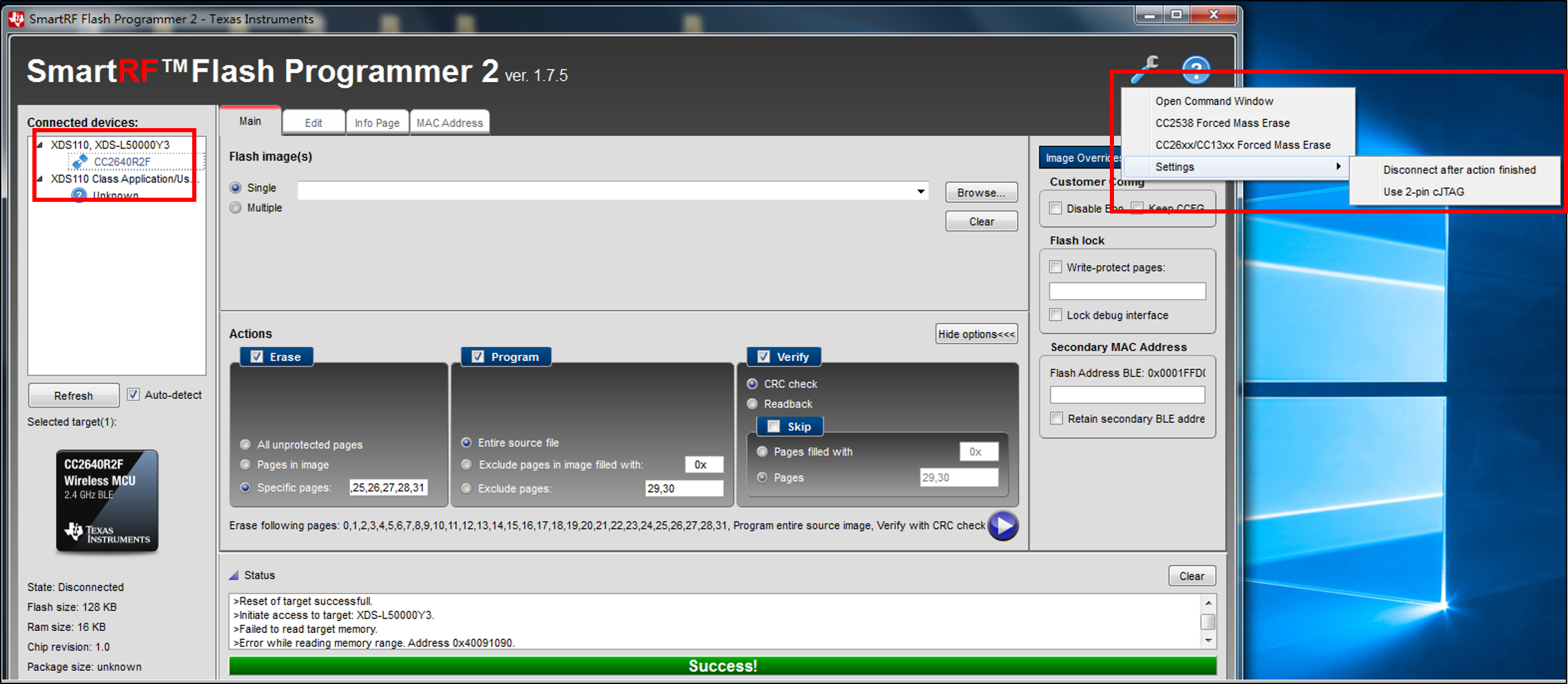
My debug interface of CC2640 is locked , as shown in picture 1 .
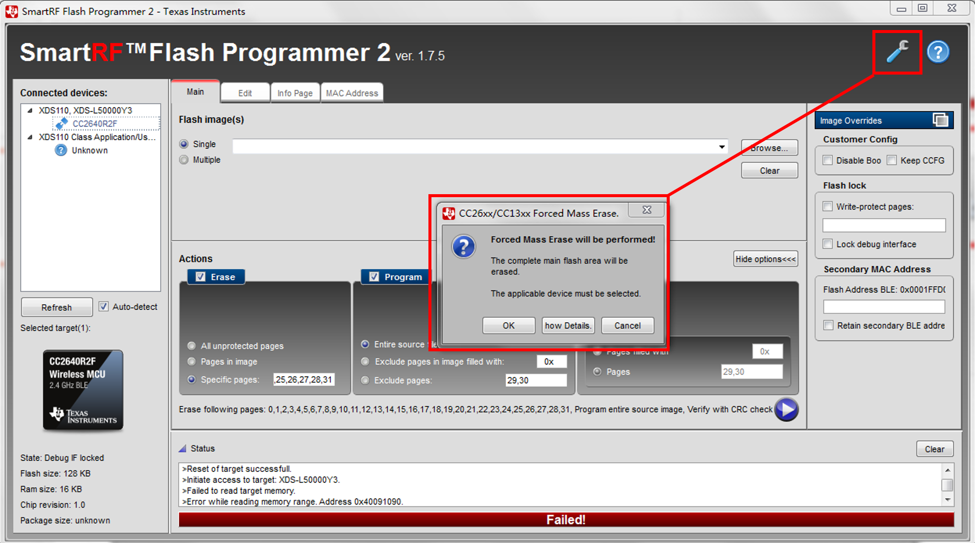
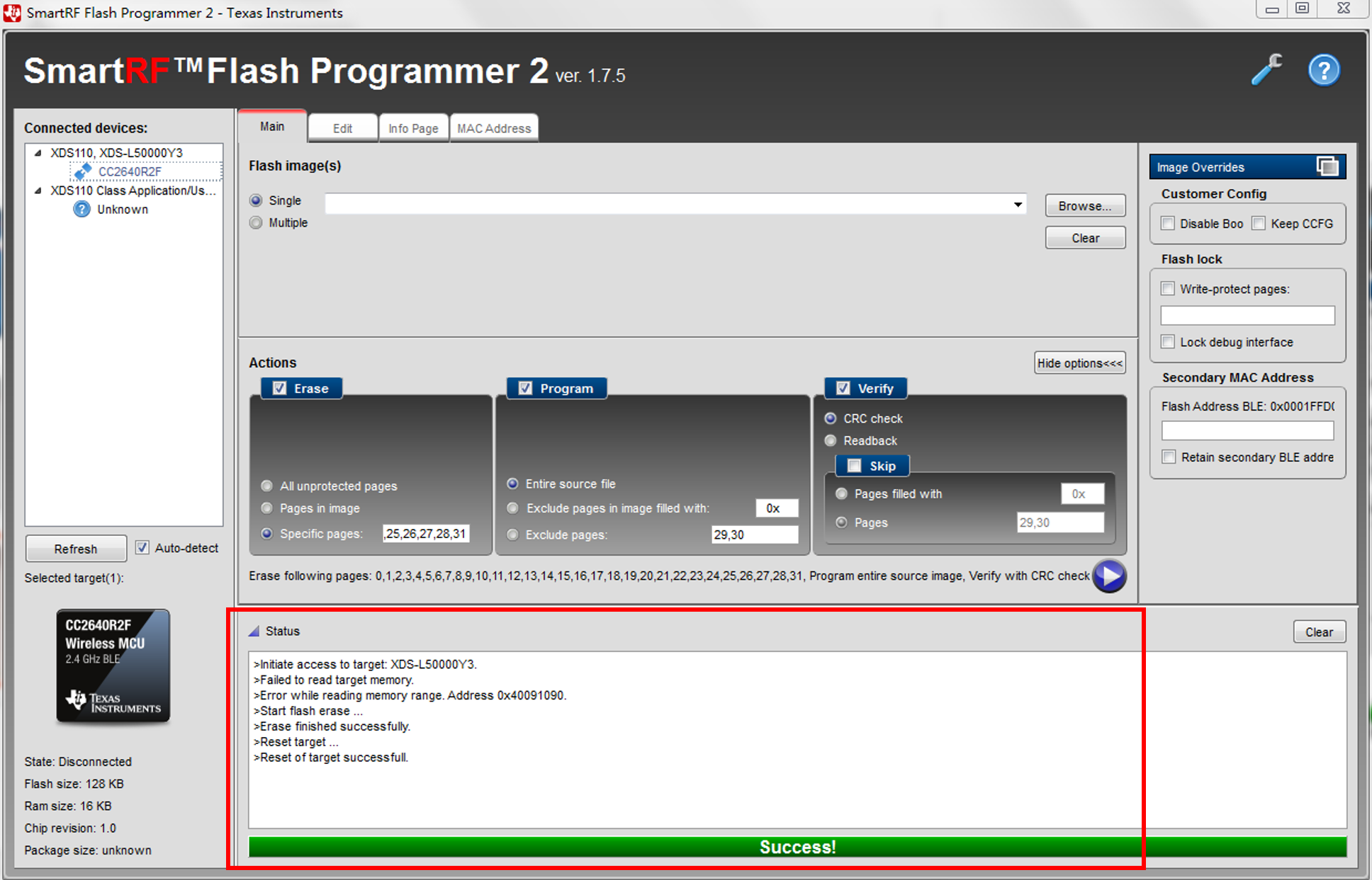
The CC2640 was programmed with my own bootloader programme . The serial port is UART ,and the bauderate is 115200. However , after more than 100 times of flashing , the debug interface of CC2640 is locked . In order to unlock the debug interface , the latest smart flash programmer was installed , as shown in picture 2 .
How to unlock the debug interface with smart flash programmer ?
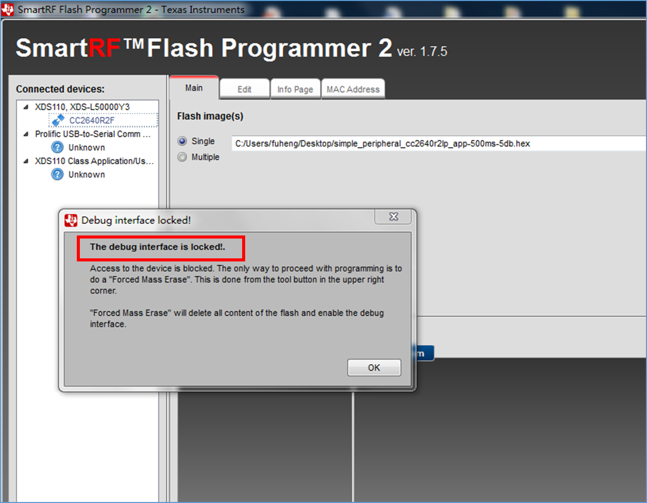
picture 1
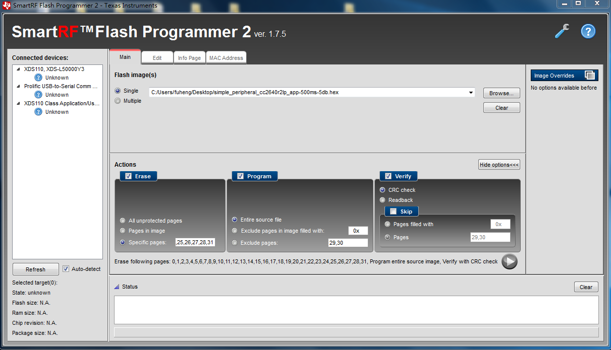
picture 2
1.Attachments:
[1]my CC2640R2 launchpad is bought from here::
www.ti.com/.../launchxl-cc2640r2
2.My develop environment:
[1]CCS:Code Composer Studio 7.2.0
[2]SDK:simplelink_cc2640r2_sdk_1_40_00_45
[3]hardware:CC26640R2 launchpad develop kit
[4]smart flash programmer 2 ver.1.7.5