This thread has been locked.

If you have a related question, please click the "Ask a related question" button in the top right corner. The newly created question will be automatically linked to this question.

CCS/TM4C1290NCPDT: Interfacing ADC - AD7177-2 with TM4C129

Part Number: TM4C129ENCPDT
Other Parts Discussed in Thread: EK-TM4C1294XL, TM4C1290NCPDT, , EK-TM4C129EXL

Tool/software: Code Composer Studio

Experience Level: Beginner

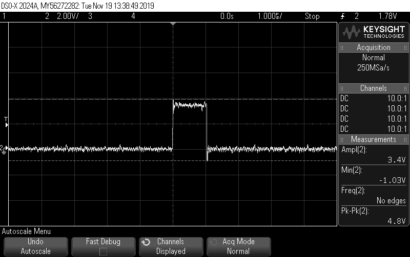
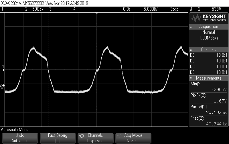
Trying to establish communication between ADC and  controller via SPI. 

Data sheet of the ADC - https://www.analog.com/media/en/technical-documentation/data-sheets/AD7177-2.pdf

As per the data sheet, the command should be given to Communications register and its given that the best way to check if both the devices are communicating is by reading the ID Register ( Reference: Pg- 49,55)

According to that, I'm expecting to read 0x4FDX (Please correct me I'm wrong)

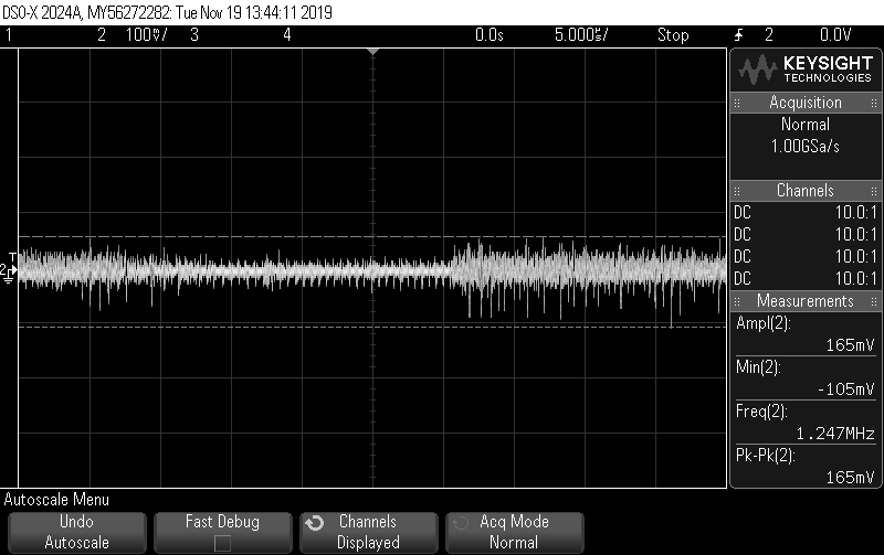
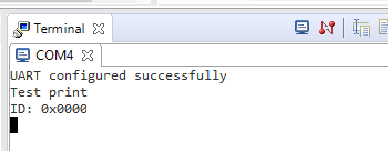
But I'm reading random values like : "128", "0", "255".

(Tried ways like using GPIO Interuppt, changing the filter configuration etc)

Struck here for over a week now. Not able to understand where I'm going wrong. Any help so as how I move forward is highly appreciated. Thanks!

Following is the source code: 

#include <stdbool.h>
#include <stdint.h>
#include "inc/hw_memmap.h"
#include "driverlib/gpio.h"
#include "driverlib/pin_map.h"
#include "driverlib/ssi.h"
#include "driverlib/sysctl.h"
#include "driverlib/uart.h"
#include "utils/uartstdio.h"
#include "inc/hw_types.h"
#include "inc/hw_ints.h"
#include "driverlib/adc.h"
#include "driverlib/interrupt.h"
#include "driverlib/rom.h"
#include "driverlib/rom_map.h"
#include "driverlib/fpu.h"
#include "driverlib/debug.h"
#include "drivers/pinout.h"


//*****************************************************************************
//
//! \addtogroup ssi_examples_list
//! <h1>SPI Master (spi_master)</h1>
//!
//! This example shows how to configure the SSI0 as SPI Master. The code will
//! send three characters on the master Tx then polls the receive FIFO until
//! 3 characters are received on the master Rx.
//!
//! This example uses the following peripherals and I/O signals. You must
//! review these and change as needed for your own board:
//! - SSI0 peripheral
//! - GPIO Port A peripheral (for SSI0 pins)
//! - SSI0Clk - PA2
//! - SSI0Fss - PA3 (Tried connecting it to ground as well)
//! - SSI0Rx - PA4
//! - SSI0Tx - PA5
//!
//! The following UART signals are configured only for displaying console
//! messages for this example. These are not required for operation of SSI0.
//! - UART0 peripheral
//! - GPIO Port A peripheral (for UART0 pins)
//! - UART0RX - PA0
//! - UART0TX - PA1
//!
//! This example uses the following interrupt handlers. To use this example
//! in your own application you must add these interrupt handlers to your
//! vector table.
//! - None.
//
//*****************************************************************************

//*****************************************************************************
//
// Number of bytes to send and receive.
//
//*****************************************************************************
#define NUM_SSI_DATA 4
uint32_t g_ui32SysClock;
uint32_t pui32DataRx[2];
uint32_t pui32DataRx_1[NUM_SSI_DATA];
uint32_t pui32DataTx_1[NUM_SSI_DATA];
uint32_t ui32Index;
uint32_t *temp;
//*****************************************************************************
//
// This function sets up UART0 to be used for a console to display information
// as the example is running.
//
//*****************************************************************************

//void IntSR();

void ConfigureUART(void)
{
//
// Enable the GPIO Peripheral used by the UART.
//
ROM_SysCtlPeripheralEnable(SYSCTL_PERIPH_GPIOA);

//
// Enable UART0
//
ROM_SysCtlPeripheralEnable(SYSCTL_PERIPH_UART0);

//
// Configure GPIO Pins for UART mode.
//
ROM_GPIOPinConfigure(GPIO_PA0_U0RX);
ROM_GPIOPinConfigure(GPIO_PA1_U0TX);
ROM_GPIOPinTypeUART(GPIO_PORTA_BASE, GPIO_PIN_0 | GPIO_PIN_1);

//
// Initialize the UART for console I/O.
//
UARTStdioConfig(0, 115200, g_ui32SysClock);
UARTprintf("UART configured successfully\n");
}


//*****************************************************************************
//
// Configure SSI0 in master Freescale (SPI) mode. This example will send out
// 3 bytes of data, then wait for 3 bytes of data to come in. This will all be
// done using the polling method.
//
//*****************************************************************************
void
main(void)
{
ConfigureUART();

/*
#if defined(TARGET_IS_TM4C129_RA0) || \
defined(TARGET_IS_TM4C129_RA1) || \
defined(TARGET_IS_TM4C129_RA2)
uint32_t ui32SysClock;
#endif
*/
g_ui32SysClock = MAP_SysCtlClockFreqSet((SYSCTL_XTAL_25MHZ |
SYSCTL_OSC_MAIN | SYSCTL_USE_PLL |
SYSCTL_CFG_VCO_480), 120000000);//Sets the clock Frequency

// PinoutSet(false, false);//enables the GPIO modules and configures the device pins for standard usages

// Display the setup on the console.

// UARTprintf("SSI ->\n");
// UARTprintf(" Mode: SPI\n");
// UARTprintf(" Data: 8-bit\n\n");

//
// The SSI0 peripheral must be enabled for use.
//

SysCtlPeripheralEnable(SYSCTL_PERIPH_SSI0);

//
// For this example SSI0 is used with PortA[5:2]. The actual port and pins
// used may be different on your part, consult the data sheet for more
// information. GPIO port A needs to be enabled so these pins can be used.
// TODO: change this to whichever GPIO port you are using.
//
// SysCtlPeripheralEnable(SYSCTL_PERIPH_GPIOA);

//
// Configure the pin muxing for SSI0 functions on port A2, A3, A4, and A5.
// This step is not necessary if your part does not support pin muxing.
// TODO: change this to select the port/pin you are using.
//
GPIOPinConfigure(GPIO_PA2_SSI0CLK);
GPIOPinConfigure(GPIO_PA3_SSI0FSS);
GPIOPinConfigure(GPIO_PA5_SSI0XDAT1);
GPIOPinConfigure(GPIO_PA4_SSI0XDAT0);

// //GPIOIntRegisterPin(GPIO_PORTB_BASE, GPIO_PIN_3, ISR);
// GPIOPinTypeGPIOOutput(GPIO_PORTA_BASE, GPIO_PIN_3);
// GPIOPinWrite(GPIO_PORTA_BASE,GPIO_PIN_3, 0);
//GPIOPinTypeGPIOInput(GPIO_PORTB_BASE, GPIO_PIN_2);


//
// Configure the GPIO settings for the SSI pins. This function also gives
// control of these pins to the SSI hardware. Consult the data sheet to
// see which functions are allocated per pin.
// The pins are assigned as follows:
// PA5 - SSI0Tx
// PA4 - SSI0Rx
// PA3 - SSI0Fss
// PA2 - SSI0CLK
// TODO: change this to select the port/pin you are using.
//
GPIOPinTypeSSI(GPIO_PORTA_BASE, GPIO_PIN_5 | GPIO_PIN_4 | GPIO_PIN_3 |
GPIO_PIN_2);

//
// Configure and enable the SSI port for SPI master mode. Use SSI0,
// system clock supply, idle clock level low and active low clock in
// freescale SPI mode, master mode, 1MHz SSI frequency, and 8-bit data.
// For SPI mode, you can set the polarity of the SSI clock when the SSI
// unit is idle. You can also configure what clock edge you want to
// capture data on. Please reference the datasheet for more information on
// the different SPI modes.
//
#if defined(TARGET_IS_TM4C129_RA0) || \
defined(TARGET_IS_TM4C129_RA1) || \
defined(TARGET_IS_TM4C129_RA2)
SSIConfigSetExpClk(SSI0_BASE, g_ui32SysClock, SSI_FRF_MOTO_MODE_1,
SSI_MODE_MASTER, 300000, 8);
#else
SSIConfigSetExpClk(SSI0_BASE,g_ui32SysClock , SSI_FRF_MOTO_MODE_1,
SSI_MODE_MASTER, 300000, 8);
#endif

//UARTprintf("Test print \n");
//
// Enable the SSI0 module.
//
//SSIAdvModeSet(SSI0_BASE, SSI_ADV_MODE_QUAD_WRITE);
SSIAdvModeSet(SSI0_BASE, SSI_ADV_MODE_READ_WRITE);
SSIEnable(SSI0_BASE);
SSIDataPut(SSI0_BASE,0x47);//Command word To read ID register
while(SSIDataGetNonBlocking(SSI0_BASE, &pui32DataRx[0]))
{
}
// SSIDataPut(SSI0_BASE,0x8274);
//
//ox29 -> Fliter Config 1
//Filter - Sinc3 -> Bit word= 1000001001101000 = 0x8268
//Filter - Sinc3 -> Bit word= 1000001001110100 =
int a=1;
SSIDataPut(SSI0_BASE,0x0047);
while(SSIBusy(SSI0_BASE))
{
}


// for(ui32Index = 0; ui32Index < 2; ui32Index++)
// {
//
// //
// // Receive the data using the "blocking" Get function. This function
// // will wait until there is data in the receive FIFO before returning.
// //
// SSIDataGet(SSI0_BASE, &pui32DataRx[ui32Index]);
// //UARTprintf("Test print\n");
// //
// // Since we are using 8-bit data, mask off the MSB.
// //
// pui32DataRx[ui32Index] &= 0x000000FF;
//
// //
// // Display the data that SSI0 received.
// //
// // UARTprintf("Received = ");
// // UARTprintf("'%d' ", pui32DataRx[ui32Index]);
// while(SSIBusy(SSI0_BASE))
// {
// }
//
// }

// while(SSIBusy(SSI0_BASE))
// {
// }

//
// Read any residual data from the SSI port. This makes sure the receive
// FIFOs are empty, so we don't read any unwanted junk. This is done here
// because the SPI SSI mode is full-duplex, which allows you to send and
// receive at the same time. The SSIDataGetNonBlocking function returns
// "true" when data was returned, and "false" when no data was returned.
// The "non-blocking" function checks if there is any data in the receive
// FIFO and does not "hang" if there isn't.
//

// GPIOPinTypeGPIOInput(GPIO_PORTP_BASE, GPIO_PIN_0);
// GPIOIntTypeSet(GPIO_PORTP_BASE, GPIO_PIN_0, GPIO_FALLING_EDGE);
// GPIOIntEnable(GPIO_PORTP_BASE, GPIO_PIN_0);
// IntEnable(INT_GPIOP0);

// GPIOIntTypeSet(GPIO_PORTA_BASE, GPIO_PIN_4, GPIO_FALLING_EDGE);
// GPIOIntEnable(GPIO_PORTA_BASE, GPIO_PIN_4);
// IntEnable(INT_GPIOA);
//IntTrigger(INT_GPIOP0);
//UARTprintf("Interrupt configured successfully\n");


//
// Display indication that the SSI is transmitting data.
//


//UARTprintf("'%d' ", *temp);
//UARTprintf("Sent:\n ");
//SSIDataGet(SSI0_BASE, &pui32DataRx[ui32Index]);

//
// Wait until SSI0 is done transferring all the data in the transmit FIFO.
//


//
// Display indication that the SSI is receiving data.
//
// UARTprintf("\nInterrupt not occurred\n ");

//
// Receive 3 bytes of data.
//
for(ui32Index = 0; ui32Index < NUM_SSI_DATA; ui32Index++)
{
//
// Receive the data using the "blocking" Get function. This function
// will wait until there is data in the receive FIFO before returning.
//
SSIDataGet(SSI0_BASE, &pui32DataRx[ui32Index]);

//
// Since we are using 8-bit data, mask off the MSB.
//
pui32DataRx[ui32Index] &= 0x000000FF;

//
// Display the data that SSI0 received.
//
UARTprintf("'%d' ", pui32DataRx[ui32Index]);
while(SSIBusy(SSI0_BASE))
{
}
}

while(1)
{
//UARTprintf("Idle state\n");
}

//
// Return no errors
//
//return(0);*/
}
/*
void ISR()
{
GPIOIntClear(GPIO_PORTA_BASE,GPIO_PIN_4);
//UARTprintf("Interrupt Occurred\n");
//SSIDataGet(SSI0_BASE, &pui32DataRx[ui32Index]);

// while(SSIDataGetNonBlocking(SSI0_BASE, &pui32DataRx_1[0]))
// {
// }

// SSIDataPut(SSI0_BASE,0x00);
// while(SSIBusy(SSI0_BASE))
// {
// }
SSIDataPut(SSI0_BASE,0x44);
while(SSIBusy(SSI0_BASE))
{
}
for(ui32Index = 0; ui32Index < NUM_SSI_DATA; ui32Index++)
{

//
// Receive the data using the "blocking" Get function. This function
// will wait until there is data in the receive FIFO before returning.
//
SSIDataGet(SSI0_BASE, &pui32DataRx_1[ui32Index]);
//UARTprintf("Test print\n");
//
// Since we are using 8-bit data, mask off the MSB.
//
pui32DataRx_1[ui32Index] &= 0x000000FF;

//
// Display the data that SSI0 received.
//
// UARTprintf("Received = ");
// UARTprintf("'%d' ", pui32DataRx[ui32Index]);
while(SSIBusy(SSI0_BASE))
{
}

}


}
*/

  • Without spending a lot of time learning my competitor's ADC and debugging your code, it looks to me like you should be using SSI_FRF_MOTO_MODE_3. I suggest that you use a logic analyzer or digital scope to capture the SSI waveform. From that picture we will be able to tell what is going on.

  • Dear Bob,

    Thanks for your response. As per your suggestion, I have configured it using SSI_FRF_MOTO_MODE_3. But there doesn't seem to be much of a difference in the waveform. I'm attaching the screenshot of DOUT from DSO.

     f DOUT 

    Any leads would be helpful.

    Regards,

    Pranav 

  • Unfortunately that does not help me much. I would like to see the waveforms of PA2, PA3, PA4 and PA5 all at the same time. (SSI0CLK, SSI0FSS, SSI0TX and SSI0RX). It is the relationship between these signals that tells me if the SSI is configured properly.

  • Dear Bob,

    Thanks for your prompt response. As per your advice, I'm attaching the screenshots of all 4 pins. What do u think is the issue?

    (Din,Dout,Fss, Sclk - same order)

  • That does not look right at all. I will try your code one my EK-TM4C1294XL launchpad, but I don't have the AD7177-2. Please post the schematic showing how you connected the TM4C1290 to the AD7177-2.

  • Ok, first you need to move the call to ConfgureUART() to after the call to MAP_SysCtlClockFreqSet(). ConfigureUART uses the variable g_ui32SysClock which is initialized by MAP_SysCtlClockFreqSet().

    Second, the address of the ID register is 0x07, not 0x47.

    Finally, each SSI transfer is both a transmit and receive. All transfers are initiated by the master, in this case the TM4C. Each SSIDataPut() should have an SSIDataGet() even if the received data is dummy. To read back from the slave you need an SSIDataPut() to start the transfer, even if the data you write is don't care.

    I modified your original code like this: (note: I used the </> button to insert the code with formatting)

    #include <stdbool.h>
    #include <stdint.h>
    #include "inc/hw_memmap.h"
    #include "driverlib/gpio.h"
    #include "driverlib/pin_map.h"
    #include "driverlib/ssi.h"
    #include "driverlib/sysctl.h"
    #include "driverlib/uart.h"
    #include "utils/uartstdio.h"
    #include "inc/hw_types.h"
    #include "inc/hw_ints.h"
    #include "driverlib/adc.h"
    #include "driverlib/interrupt.h"
    #include "driverlib/rom.h"
    #include "driverlib/rom_map.h"
    #include "driverlib/fpu.h"
    #include "driverlib/debug.h"
    #include "drivers/pinout.h"
    
    
    //*****************************************************************************
    //
    //! \addtogroup ssi_examples_list
    //! <h1>SPI Master (spi_master)</h1>
    //!
    //! This example shows how to configure the SSI0 as SPI Master. The code will
    //! send three characters on the master Tx then polls the receive FIFO until
    //! 3 characters are received on the master Rx.
    //!
    //! This example uses the following peripherals and I/O signals. You must
    //! review these and change as needed for your own board:
    //! - SSI0 peripheral
    //! - GPIO Port A peripheral (for SSI0 pins)
    //! - SSI0Clk - PA2
    //! - SSI0Fss - PA3 (Tried connecting it to ground as well)
    //! - SSI0Rx - PA4
    //! - SSI0Tx - PA5
    //!
    //! The following UART signals are configured only for displaying console
    //! messages for this example. These are not required for operation of SSI0.
    //! - UART0 peripheral
    //! - GPIO Port A peripheral (for UART0 pins)
    //! - UART0RX - PA0
    //! - UART0TX - PA1
    //!
    //! This example uses the following interrupt handlers. To use this example
    //! in your own application you must add these interrupt handlers to your
    //! vector table.
    //! - None.
    //
    //*****************************************************************************
    
    //*****************************************************************************
    //
    // Number of bytes to send and receive.
    //
    //*****************************************************************************
    #define NUM_SSI_DATA 4
    uint32_t g_ui32SysClock;
    uint32_t pui32DataRx[2];
    uint32_t pui32DataRx_1[NUM_SSI_DATA];
    uint32_t pui32DataTx_1[NUM_SSI_DATA];
    uint32_t ui32Index;
    uint32_t *temp;
    //*****************************************************************************
    //
    // This function sets up UART0 to be used for a console to display information
    // as the example is running.
    //
    //*****************************************************************************
    
    //void IntSR();
    
    void ConfigureUART(void)
    {
        //
        // Enable the GPIO Peripheral used by the UART.
        //
        ROM_SysCtlPeripheralEnable(SYSCTL_PERIPH_GPIOA);
    
        //
        // Enable UART0
        //
        ROM_SysCtlPeripheralEnable(SYSCTL_PERIPH_UART0);
    
        //
        // Configure GPIO Pins for UART mode.
        //
        ROM_GPIOPinConfigure(GPIO_PA0_U0RX);
        ROM_GPIOPinConfigure(GPIO_PA1_U0TX);
        ROM_GPIOPinTypeUART(GPIO_PORTA_BASE, GPIO_PIN_0 | GPIO_PIN_1);
    
        //
        // Initialize the UART for console I/O.
        //
        UARTStdioConfig(0, 115200, g_ui32SysClock);
        UARTprintf("UART configured successfully\n");
    }
    
    
    //*****************************************************************************
    //
    // Configure SSI0 in master Freescale (SPI) mode. This example will send out
    // 3 bytes of data, then wait for 3 bytes of data to come in. This will all be
    // done using the polling method.
    //
    //*****************************************************************************
    void
    main(void)
    {
    
        /*
        #if defined(TARGET_IS_TM4C129_RA0) || \
        defined(TARGET_IS_TM4C129_RA1) || \
        defined(TARGET_IS_TM4C129_RA2)
        uint32_t ui32SysClock;
        #endif
        */
        g_ui32SysClock = MAP_SysCtlClockFreqSet((SYSCTL_XTAL_25MHZ |
            SYSCTL_OSC_MAIN | SYSCTL_USE_PLL |
            SYSCTL_CFG_VCO_480), 120000000);//Sets the clock Frequency
    
        ConfigureUART();
        // PinoutSet(false, false);//enables the GPIO modules and configures the device pins for standard usages
    
        // Display the setup on the console.
    
        // UARTprintf("SSI ->\n");
        // UARTprintf(" Mode: SPI\n");
        // UARTprintf(" Data: 8-bit\n\n");
    
        //
        // The SSI0 peripheral must be enabled for use.
        //
    
        SysCtlPeripheralEnable(SYSCTL_PERIPH_SSI0);
    
        //
        // For this example SSI0 is used with PortA[5:2]. The actual port and pins
        // used may be different on your part, consult the data sheet for more
        // information. GPIO port A needs to be enabled so these pins can be used.
        // TODO: change this to whichever GPIO port you are using.
        //
        // SysCtlPeripheralEnable(SYSCTL_PERIPH_GPIOA);
    
        //
        // Configure the pin muxing for SSI0 functions on port A2, A3, A4, and A5.
        // This step is not necessary if your part does not support pin muxing.
        // TODO: change this to select the port/pin you are using.
        //
        GPIOPinConfigure(GPIO_PA2_SSI0CLK);
        GPIOPinConfigure(GPIO_PA3_SSI0FSS);
        GPIOPinConfigure(GPIO_PA5_SSI0XDAT1);
        GPIOPinConfigure(GPIO_PA4_SSI0XDAT0);
    
        // //GPIOIntRegisterPin(GPIO_PORTB_BASE, GPIO_PIN_3, ISR);
        // GPIOPinTypeGPIOOutput(GPIO_PORTA_BASE, GPIO_PIN_3);
        // GPIOPinWrite(GPIO_PORTA_BASE,GPIO_PIN_3, 0);
        //GPIOPinTypeGPIOInput(GPIO_PORTB_BASE, GPIO_PIN_2);
    
    
        //
        // Configure the GPIO settings for the SSI pins. This function also gives
        // control of these pins to the SSI hardware. Consult the data sheet to
        // see which functions are allocated per pin.
        // The pins are assigned as follows:
        // PA5 - SSI0Tx
        // PA4 - SSI0Rx
        // PA3 - SSI0Fss
        // PA2 - SSI0CLK
        // TODO: change this to select the port/pin you are using.
        //
        GPIOPinTypeSSI(GPIO_PORTA_BASE, GPIO_PIN_5 | GPIO_PIN_4 | GPIO_PIN_3 |
            GPIO_PIN_2);
    
        //
        // Configure and enable the SSI port for SPI master mode. Use SSI0,
        // system clock supply, idle clock level low and active low clock in
        // freescale SPI mode, master mode, 1MHz SSI frequency, and 8-bit data.
        // For SPI mode, you can set the polarity of the SSI clock when the SSI
        // unit is idle. You can also configure what clock edge you want to
        // capture data on. Please reference the datasheet for more information on
        // the different SPI modes.
        //
        SSIConfigSetExpClk(SSI0_BASE, g_ui32SysClock, SSI_FRF_MOTO_MODE_3,
            SSI_MODE_MASTER, 300000, 8);
    
        //
        // Enable the SSI0 module.
        //
        //SSIAdvModeSet(SSI0_BASE, SSI_ADV_MODE_QUAD_WRITE);
        SSIAdvModeSet(SSI0_BASE, SSI_ADV_MODE_READ_WRITE);
        SSIEnable(SSI0_BASE);
        // Make sure receive FIFO is empty
        while(SSIDataGetNonBlocking(SSI0_BASE, &pui32DataRx[0]))
        {
        }
    
        UARTprintf("Test print \n");
    
        SSIDataPut(SSI0_BASE,0x07);//Command word To read ID register
        SSIDataGet(SSI0_BASE,pui32DataRx); // dummy data
        // Now read the two bytes of the ID
        SSIDataPut(SSI0_BASE,0x00);//send dummy data
        SSIDataGet(SSI0_BASE,&pui32DataRx[0]); // first byte
        SSIDataPut(SSI0_BASE,0x00);//send dummy data
        SSIDataGet(SSI0_BASE,&pui32DataRx[1]); // second byte
    
        //
        // Print the 2 bytes (16-bit) value received.
        //
        UARTprintf("ID: 0x%02x%02x\n", pui32DataRx[0], pui32DataRx[1]);
    
        while(1)
        {
        //UARTprintf("Idle state\n");
        }
    
        //
        // Return no errors
        //
        //return(0);*/
    }
    

    Here is what the SSI pins look like using a logic analyzer. Remember that I don't have an AD7177-2 chip attached so I get 0s where you should get 0x4FDx.

    Here is the output I received in Terminal:

  • Double check your connections:

    TM4C                        AD7177-2

    CLK-PA2         to       SCLK 

    SSITX - PA4    to       DIN

    SSIRX - PA5   to        DOUT/RDY (corrected 20-Nov-2019)

    FSS - PA3       to        CS-    

  • Dear Bob,

    Thank you for spending your valuable time. I tried again with your code but didn't succeed. Circuit connected is as follows:

    PA2 - SCLK

    PA4 - DIN

    PA5 - DOUT (As per the configuration lines in code it should be connected to PA5) (Please correct me if I'm wrong)

    PA3 - CS

     I read 0xffff most of the times. Rarely I read 0x0000

    Scope shots of DIN, DOUT, SCLK and CS in the same order.

    What do you think is going wrong here?


  • The power connections are as follows:

    AVSS - GND

    AVDD1 - 5V

    AVDD2 - AVDD1 (as per the data sheet - pg:19)

    IOVDD - 3V3

    DGND - GND

  • Yes, PA5 should be connected to DOUT. (I have corrected my typo in the post above.)

    Your scope pictures don't match my logic analyzer image at all. Do you have a 25MHz crystal attached to the TM4C1290NCPDT? Can you try running the code I provided without any connections to the AD7177-2? Do you have two scope probes? Can you get a single scope image with both PA2 (CLK) and PA4 (SSITX)? Make sure you have a good ground connection on the scope probes.

  • I beg your pardon. I made a huge mistake while posting. I'm using TM4C129ENCPDT on an EK-TM4C1294XL dev. board. I totally apologize for my negligence in over looking the part numbers. 

    What do you think are the key differences ? 

  • Should be no difference at all. The code I sent you was tested on a TM4C129ENCPDT on an EK-TM4C129EXL launchpad. Run the code I sent you on your launchpad without the AD7177-2 attached and verify you get signals like the logic analyzer image I posted.

  • Dear Bob,

    Firstly many thanks for your prompt responses. Your code does work. I've got the desired output. Thank you so much. I've been struggling with it for over 3 weeks now.

    2 key things to sum up the forum discussion: 

    1) I was sending you the scope shots after all the configuration, transmission and receiving was done i.e., (when the code was running in while(1) ), so obviously the scope shots of your logic analyzer of mine didn't match mine. I put the config lines in a loop and tested. The SCLK, TX, CS were similar to your pictures. However RX was a little different(maybe because data was being transmitted from ADC)

    2) The command word to read ID register is 0x47. 0x07 is the command word to write to ID register. However ID register is a read only register and to read its value the command word is 0x47. (Reference - Data Sheet Pg: 49) [That was the only change I made to your code and I read 0x4DE

    Once again, thank you so much Bob. 

    Regards,

    Pranav Deep.I