This thread has been locked.

If you have a related question, please click the "Ask a related question" button in the top right corner. The newly created question will be automatically linked to this question.

CCS/TMS570LS3137-EP: TMS570LS3137

Part Number: TMS570LS3137-EP
Other Parts Discussed in Thread: RM48L952, TMS570LS3137, HALCOGEN, MSP430FR6989

Tool/software: Code Composer Studio

Hi,

In my Project, we are using RM48L952 AND TMS570LS3137 board, i required to store some important data in Flash memory of both the board. 

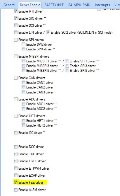
Can you please provide me a generic flash driver file which i can perform operation over the internal flash .

kindly help me, i waiting for your reply soon

Regards,

Anand Kumar NS

  • Hello Anand,

    Those Hercules devices have non-volatile flash for instruction execution or data storage. The flash bank 0 and bank 2 are used as program flash, and bank 7 is used as emulated EEPROM (FEE). EEPROM is erasable by the word while this Flash memory is only erasable by the sector. 

    The FEE is supported by HALCOGen. The HALCoGen contains a example of using FEE driver generated by HALCOGen.

  • If you want to store the data to one flash sector in Bank 0 or Bank 1, you need to use F021 flash API to program the data to flash:

    https://www.ti.com/tool/F021FLASHAPI

  • Hi QJ Wang,

    Thanks for your reply....

    I will go through once and let you know if i face any problem.

    Thanks once again.

    Regards,

    Anand Kumar NS

  • Hello Wang,

    I am using FEE_write_read driver code. In that i am facing issue that ,

    /* Write the block into EEP Synchronously. Write will not happen since data is same. */
    TI_Fee_WriteSync(BlockNumber, &SpecialRamBlock[0]);

    using the above write function . data is written into EEPROM . But it stored in @(0xF0200020 - 8) location and for every new data write, it is taking 32 bytes increment  @(0xF0200040 - 8) location.

    Can you please explain me  why it is like that.

    Using the Fee_read function i can able to read the data.

    TI_Fee_Read(BlockNumber,BlockOffset,Read_Ptr,Length);

    In my CCS IDE, Debug-->Flash setting--> unchecked for Bank 7 all the 4 Sectors so it wont erase.

    I have comment write portion of code after written once and tried to read back but data is not coming...

    Kindly help me to solve this issue .

  • Hi,

    The Data Block is to define the location of the data. The data block consists of header and data. The header takes 24-bytes. The smallest amount of data that can be stored within the Data Block is 64 bits. The minimum length of a data block is 24 bytes + 8 bytes = 32 bytes. If the Data size exceeds 64 bits, the Data Packets are added in 64 bit increments.

    If Checksum is enabled, during writing of a block, Checksum of the data to be written is calculated and checked against the Checksum of the same block which is already existing in Flash. If Checksum matches, data is not written. If Checksum is not enabled, then data is compared byte by byte. If data does not match, write will be initiated.

  • Hello Wang,

    Thanks for explaining, I have understood now it consume 32 bytes of frame in that 24 byte is header and 8 bytes is data.

    I have tried to read the data without write. but i monitored in memory window data is present. but cannot able to read the expected data. why it is like that?

    Can you please explain me, where i am making mistake. 

    steps i followed to check

    1. Required Data is written into flash bank 7,sector 0

    2. Commented the write portion of code and disable the erase option in ccs ide.

    3.  I tried to read the stored data, but data is not coming. (where i am making mistake). This is the function i am using to read the stored data

    TI_Fee_Read(BlockNumber,BlockOffset,Read_Ptr,Length); 

    Below code i am using ,

    #define WRITE_SIZE 16

    void FRAMWrite(void);

    unsigned char count = 0;
    unsigned long data;

    #if defined(__TI_COMPILER_VERSION__)
    #pragma NOINIT(FRAM_write)
    uint8_t FRAM_write[WRITE_SIZE];
    #elif defined(__IAR_SYSTEMS_ICC__)
    __persistent unsigned long FRAM_write[WRITE_SIZE] = {0};
    #elif defined(__GNUC__)
    unsigned long __attribute__((persistent)) FRAM_write[WRITE_SIZE] = {0};
    #else
    #error Compiler not supported!
    #endif

    int main(void)
    {
    WDTCTL = WDTPW | WDTHOLD; // Stop WDT

    // Configure GPIO
    P1OUT &= ~BIT0; // Clear P1.0 output latch for a defined power-on state
    P1DIR |= BIT0; // Set P1.0 to output direction

    // Disable the GPIO power-on default high-impedance mode to activate
    // previously configured port settings
    PM5CTL0 &= ~LOCKLPM5;

    // Initialize dummy data
    data = 0x00010001;

    while(1)
    {
    data += 0x00010001;
    FRAMWrite();
    count++;
    //if (count > 100)
    {
    P1OUT ^= 0x01; // Toggle LED to show 512K bytes
    count = 0; // ..have been written
    // data = 0x00010001;
    }
    }
    }

    void FRAMWrite(void)
    {
    unsigned int i=0;

    for ( i= 0; i< 16; i++)
    {
    FRAM_write[i] = data;
    }
    }

    and i have changed linker script file as 

    /* ============================================================================ */
    /* Copyright (c) 2017, Texas Instruments Incorporated */
    /* All rights reserved. */
    /* */
    /* Redistribution and use in source and binary forms, with or without */
    /* modification, are permitted provided that the following conditions */
    /* are met: */
    /* */
    /* * Redistributions of source code must retain the above copyright */
    /* notice, this list of conditions and the following disclaimer. */
    /* */
    /* * Redistributions in binary form must reproduce the above copyright */
    /* notice, this list of conditions and the following disclaimer in the */
    /* documentation and/or other materials provided with the distribution. */
    /* */
    /* * Neither the name of Texas Instruments Incorporated nor the names of */
    /* its contributors may be used to endorse or promote products derived */
    /* from this software without specific prior written permission. */
    /* */
    /* THIS SOFTWARE IS PROVIDED BY THE COPYRIGHT HOLDERS AND CONTRIBUTORS "AS IS" */
    /* AND ANY EXPRESS OR IMPLIED WARRANTIES, INCLUDING, BUT NOT LIMITED TO, */
    /* THE IMPLIED WARRANTIES OF MERCHANTABILITY AND FITNESS FOR A PARTICULAR */
    /* PURPOSE ARE DISCLAIMED. IN NO EVENT SHALL THE COPYRIGHT OWNER OR */
    /* CONTRIBUTORS BE LIABLE FOR ANY DIRECT, INDIRECT, INCIDENTAL, SPECIAL, */
    /* EXEMPLARY, OR CONSEQUENTIAL DAMAGES (INCLUDING, BUT NOT LIMITED TO, */
    /* PROCUREMENT OF SUBSTITUTE GOODS OR SERVICES; LOSS OF USE, DATA, OR PROFITS; */
    /* OR BUSINESS INTERRUPTION) HOWEVER CAUSED AND ON ANY THEORY OF LIABILITY, */
    /* WHETHER IN CONTRACT, STRICT LIABILITY, OR TORT (INCLUDING NEGLIGENCE OR */
    /* OTHERWISE) ARISING IN ANY WAY OUT OF THE USE OF THIS SOFTWARE, */
    /* EVEN IF ADVISED OF THE POSSIBILITY OF SUCH DAMAGE. */
    /* ============================================================================ */

    /******************************************************************************/
    /* lnk_msp430fr6989.cmd - LINKER COMMAND FILE FOR LINKING MSP430FR6989 PROGRAMS */
    /* */
    /* Usage: lnk430 <obj files...> -o <out file> -m <map file> lnk.cmd */
    /* cl430 <src files...> -z -o <out file> -m <map file> lnk.cmd */
    /* */
    /*----------------------------------------------------------------------------*/
    /* These linker options are for command line linking only. For IDE linking, */
    /* you should set your linker options in Project Properties */
    /* -c LINK USING C CONVENTIONS */
    /* -stack 0x0100 SOFTWARE STACK SIZE */
    /* -heap 0x0100 HEAP AREA SIZE */
    /* */
    /*----------------------------------------------------------------------------*/
    /* Version: 1.204 */
    /*----------------------------------------------------------------------------*/

    /****************************************************************************/
    /* Specify the system memory map */
    /****************************************************************************/

    MEMORY
    {
    TINYRAM : origin = 0x0006, length = 0x001A
    PERIPHERALS_8BIT : origin = 0x0020, length = 0x00E0
    PERIPHERALS_16BIT : origin = 0x0100, length = 0x0100
    RAM : origin = 0x1C00, length = 0x0800
    INFOA : origin = 0x1980, length = 0x0080
    INFOB : origin = 0x1900, length = 0x0080
    INFOC : origin = 0x1880, length = 0x0080
    INFOD : origin = 0x1800, length = 0x0080
    FRAM : origin = 0x4400, length = 0xBB80
    FRAM2 : origin = 0x10000,length = 0x14000
    JTAGSIGNATURE : origin = 0xFF80, length = 0x0004, fill = 0xFFFF
    BSLSIGNATURE : origin = 0xFF84, length = 0x0004, fill = 0xFFFF
    IPESIGNATURE : origin = 0xFF88, length = 0x0008, fill = 0xFFFF
    INT00 : origin = 0xFF90, length = 0x0002
    INT01 : origin = 0xFF92, length = 0x0002
    INT02 : origin = 0xFF94, length = 0x0002
    INT03 : origin = 0xFF96, length = 0x0002
    INT04 : origin = 0xFF98, length = 0x0002
    INT05 : origin = 0xFF9A, length = 0x0002
    INT06 : origin = 0xFF9C, length = 0x0002
    INT07 : origin = 0xFF9E, length = 0x0002
    INT08 : origin = 0xFFA0, length = 0x0002
    INT09 : origin = 0xFFA2, length = 0x0002
    INT10 : origin = 0xFFA4, length = 0x0002
    INT11 : origin = 0xFFA6, length = 0x0002
    INT12 : origin = 0xFFA8, length = 0x0002
    INT13 : origin = 0xFFAA, length = 0x0002
    INT14 : origin = 0xFFAC, length = 0x0002
    INT15 : origin = 0xFFAE, length = 0x0002
    INT16 : origin = 0xFFB0, length = 0x0002
    INT17 : origin = 0xFFB2, length = 0x0002
    INT18 : origin = 0xFFB4, length = 0x0002
    INT19 : origin = 0xFFB6, length = 0x0002
    INT20 : origin = 0xFFB8, length = 0x0002
    INT21 : origin = 0xFFBA, length = 0x0002
    INT22 : origin = 0xFFBC, length = 0x0002
    INT23 : origin = 0xFFBE, length = 0x0002
    INT24 : origin = 0xFFC0, length = 0x0002
    INT25 : origin = 0xFFC2, length = 0x0002
    INT26 : origin = 0xFFC4, length = 0x0002
    INT27 : origin = 0xFFC6, length = 0x0002
    INT28 : origin = 0xFFC8, length = 0x0002
    INT29 : origin = 0xFFCA, length = 0x0002
    INT30 : origin = 0xFFCC, length = 0x0002
    INT31 : origin = 0xFFCE, length = 0x0002
    INT32 : origin = 0xFFD0, length = 0x0002
    INT33 : origin = 0xFFD2, length = 0x0002
    INT34 : origin = 0xFFD4, length = 0x0002
    INT35 : origin = 0xFFD6, length = 0x0002
    INT36 : origin = 0xFFD8, length = 0x0002
    INT37 : origin = 0xFFDA, length = 0x0002
    INT38 : origin = 0xFFDC, length = 0x0002
    INT39 : origin = 0xFFDE, length = 0x0002
    INT40 : origin = 0xFFE0, length = 0x0002
    INT41 : origin = 0xFFE2, length = 0x0002
    INT42 : origin = 0xFFE4, length = 0x0002
    INT43 : origin = 0xFFE6, length = 0x0002
    INT44 : origin = 0xFFE8, length = 0x0002
    INT45 : origin = 0xFFEA, length = 0x0002
    INT46 : origin = 0xFFEC, length = 0x0002
    INT47 : origin = 0xFFEE, length = 0x0002
    INT48 : origin = 0xFFF0, length = 0x0002
    INT49 : origin = 0xFFF2, length = 0x0002
    INT50 : origin = 0xFFF4, length = 0x0002
    INT51 : origin = 0xFFF6, length = 0x0002
    INT52 : origin = 0xFFF8, length = 0x0002
    INT53 : origin = 0xFFFA, length = 0x0002
    INT54 : origin = 0xFFFC, length = 0x0002
    RESET : origin = 0xFFFE, length = 0x0002
    }

    /****************************************************************************/
    /* Specify the sections allocation into memory */
    /****************************************************************************/

    SECTIONS
    {
    GROUP(RW_IPE)
    {
    GROUP(READ_WRITE_MEMORY)
    {
    .TI.persistent : {} /* For #pragma persistent */
    .cio : {} /* C I/O Buffer */
    .sysmem : {} /* Dynamic memory allocation area */
    } PALIGN(0x0400), RUN_START(fram_rw_start)

    GROUP(IPENCAPSULATED_MEMORY)
    {
    .ipestruct : {} /* IPE Data structure */
    .ipe : {} /* IPE */
    .ipe_const : {} /* IPE Protected constants */
    .ipe:_isr : {} /* IPE ISRs */
    .ipe_vars : type = NOINIT{} /* IPE variables */
    } PALIGN(0x0400), RUN_START(fram_ipe_start) RUN_END(fram_ipe_end) RUN_END(fram_rx_start)
    } > 0x4400

    .cinit : {} > FRAM /* Initialization tables */
    .pinit : {} > FRAM /* C++ Constructor tables */
    .binit : {} > FRAM /* Boot-time Initialization tables */
    .init_array : {} > FRAM /* C++ Constructor tables */
    .mspabi.exidx : {} > FRAM /* C++ Constructor tables */
    .mspabi.extab : {} > FRAM /* C++ Constructor tables */
    #ifndef __LARGE_DATA_MODEL__
    .const : {} > FRAM /* Constant data */
    #else
    .const : {} >> FRAM | FRAM2 /* Constant data */
    #endif

    .text:_isr : {} > FRAM /* Code ISRs */
    #ifndef __LARGE_CODE_MODEL__
    .text : {} > FRAM /* Code */
    #else
    .text : {} >> FRAM2 | FRAM /* Code */
    #endif
    #ifdef __TI_COMPILER_VERSION__
    #if __TI_COMPILER_VERSION__ >= 15009000
    #ifndef __LARGE_CODE_MODEL__
    .TI.ramfunc : {} load=FRAM, run=RAM, table(BINIT)
    #else
    .TI.ramfunc : {} load=FRAM | FRAM2, run=RAM, table(BINIT)
    #endif
    #endif
    #endif

    .jtagsignature : {} > JTAGSIGNATURE /* JTAG Signature */
    .bslsignature : {} > BSLSIGNATURE /* BSL Signature */

    GROUP(SIGNATURE_SHAREDMEMORY)
    {
    .ipesignature : {} /* IPE Signature */
    .jtagpassword : {} /* JTAG Password */
    } > IPESIGNATURE

    .bss : {} > RAM /* Global & static vars */
    .data : {} > RAM /* Global & static vars */
    .TI.noinit : {} > FRAM /* For #pragma noinit */
    .stack : {} > RAM (HIGH) /* Software system stack */
    .tinyram : {} > TINYRAM /* Tiny RAM */

    but write to this location is not happening.....

    Thank you,

    Regards,

    Anand Kumar N S