This thread has been locked.

If you have a related question, please click the "Ask a related question" button in the top right corner. The newly created question will be automatically linked to this question.

CCS/TDA2SX: CCS9.2.0 failed to load EVE executable code

Part Number: TDA2SX
Other Parts Discussed in Thread: SYSCONFIG

Tool/software: Code Composer Studio

hi,

I am using the emulator to debug PROCESSOR_SDK_VISION_03_08_00_00.

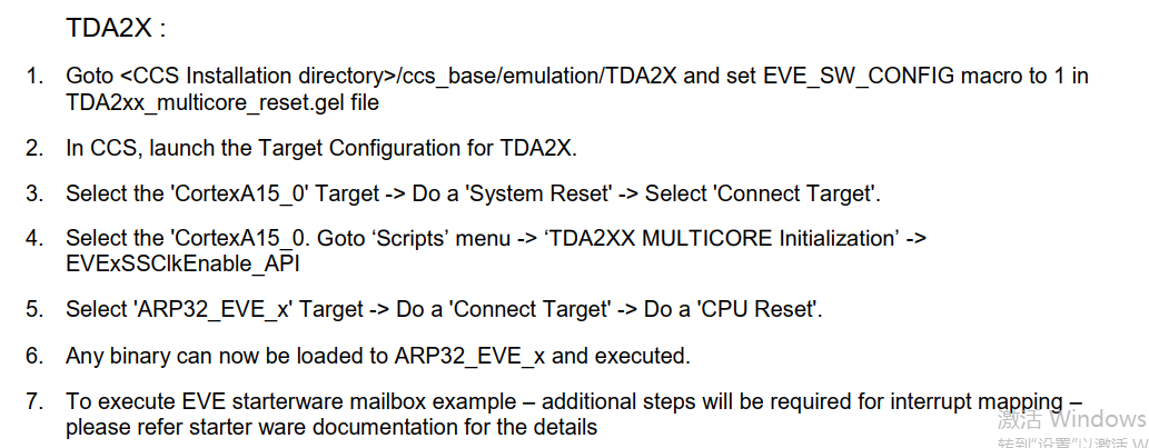
The description in the guidance document is this:

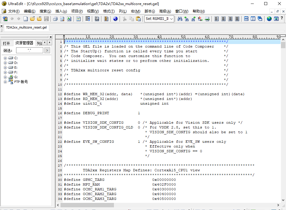
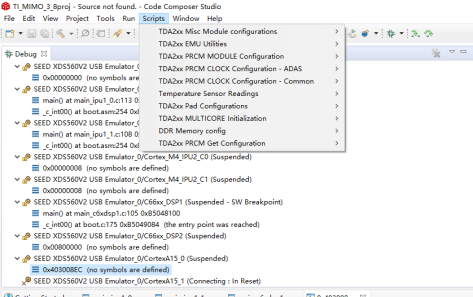
But I do not see EVE MMU config option in the Scripts menu:

there is an Error when loading the EVE executable code:

Please help me solve this problem, thank you.

  • Hi,

      Have you installed device support files for Automotive from the below location  :

    http://processors.wiki.ti.com/index.php/Device_support_files

    Regards,

    Anshu

  • Hi,

    I have installed the device support file:

    but the error still exists.

    Looking forward to your reply,thanks.

  • Hi,

      Have you followed below steps as mentioned in eve_sw_getting_started :


    Regards,

    Anshu

  • Hi Anshu,

    I did exactly the following steps:

    The problem still exists.The error message is:

    ARP32_EVE_1: Trouble Reading Memory Block at 0xb1000000 on Page 1 of Length 0x4: (Error -1065 @ 0xB1000000) Unable to access device memory. Verify that the memory address is in valid memory. If error persists, confirm configuration, power-cycle board, and/or try more reliable JTAG settings (e.g. lower TCLK). (Emulation package 8.3.0.00003)
    ARP32_EVE_1: File Loader: Verification failed: Target failed to read 0xB1000000@Data
    ARP32_EVE_1: GEL: File: D:\PROCESSOR_SDK_VISION_03_08_00_00\vision_sdk\binaries\apps\tda2xx_cascade_bios_radar\vision_sdk\bin\tda2xx-evm\vision_sdk_arp32_1_release.xearp32F: Load failed.

    Looking forward to your reply,thanks.

  • Hi, 

         Looks like some MMU configuration is not happening correctly. Can you again confirm if you have set EVE_SW_CONFIG macro to 1 in TDA2xx_multicore_reset.gel file?

    Regards,

    Anshu

  • hi Anshu,I have  set EVE_SW_CONFIG macro to 1 in TDA2xx_multicore_reset.gel file,like this.

    Thanks,waiting for your reply.

  • the error message like this,when I load code to the EVE

  • Hi,

       Can you share the following two files : 

    • "C:\ti\<ccs>\ccs_base\emulation\gel\TDA2x\TDA2xx_multicore_reset.gel"
    • Linker command file used for your application.

    Regards,

    Anshu

  • /*******************************************************************/
    /* This GEL file is loaded on the command line of Code Composer    */
    /* The StartUp() function is called every time you start           */
    /* Code Composer.  You can customize this function to              */
    /* initialize wait states or to perform other initialization.      */
    /*                                                                 */
    /* TDA2xx multicore reset config                                   */
    /*                                                                 */
    /*                                                                 */
    /*******************************************************************/
    #define WR_MEM_32(addr, data)   *(unsigned int*)(addr) =(unsigned int)(data)
    #define RD_MEM_32(addr)         *(unsigned int*)(addr)
    #define uint32_t                unsigned int
    #define DEBUG_PRINT            1
    #define VISION_SDK_CONFIG      0 /* Applicable for Vision SDK users only */
    #define VISION_SDK_CONFIG_OLD  0 /* For VSDK 2.8, set this to 1.
                                      * VISION_SDK_CONFIG should also be set to 1
                                      */
    #define EVE_SW_CONFIG          1 /* Applicable for EVE_SW users only
                                      * Effective only when
                                      * VISION_SDK_CONFIG == 0
                                      */
    /*******************************************************************************
            TDA2xx Registers Map Defines: CortexA15_CPU1 view
    *******************************************************************************/
    #define GPMC_TARG                    0x00000000
    #define MPU_RAM                      0x402F0000
    #define OCMC_RAM1_TARG               0x40300000
    #define OCMC_RAM2_TARG               0x40400000
    #define OCMC_RAM3_TARG               0x40500000
    #define DSP1_L2_SRAM_TARG            0x40800000
    #define DSP1_SYSTEM_TARG             0x40D00000
    #define DSP1_MMU0CFG_TARG            0x40D01000
    #define DSP1_MMU1CFG_TARG            0x40D02000
    #define DSP1_FW0CFG_TARG             0x40D03000
    #define DSP1_FW1CFG_TARG             0x40D04000
    #define DSP1_EDMA_TC0_TARG           0x40D05000
    #define DSP1_EDMA_TC1_TARG           0x40D06000
    #define DSP1_NoC_TARG                0x40D07000
    #define DSP1_EDMA_CC_TARG            0x40D10000
    #define DSP1_L1P_SRAM_TARG           0x40E00000
    #define DSP1_L1D_SRAM_TARG           0x40F00000
    #define DSP2_L2_SRAM_TARG            0x41000000
    #define DSP2_SYSTEM_TARG             0x41500000
    #define DSP2_MMU0CFG_TARG            0x41501000
    #define DSP2_MMU1CFG_TARG            0x41502000
    #define DSP2_FW0CFG_TARG             0x41503000
    #define DSP2_FW1CFG_TARG             0x41504000
    #define DSP2_EDMA_TC0_TARG           0x41505000
    #define DSP2_EDMA_TC1_TARG           0x41506000
    #define DSP2_NoC_TARG                0x41507000
    #define DSP2_EDMA_CC_TARG            0x41510000
    #define DSP2_L1P_SRAM_TARG           0x41600000
    #define DSP2_L1D_SRAM_TARG           0x41700000
    #define OCMC_RAM1_CBUF_TARG          0x41800000
    #define EVE1_TARG                    0x42000000
    #define EVE2_TARG                    0x42100000
    #define EVE3_TARG                    0x42200000
    #define EVE4_TARG                    0x42300000
    #define EDMA_TPCC_TARG               0x43300000
    #define EDMA_TC0_TARG                0x43400000
    #define EDMA_TC1_TARG                0x43500000
    #define OCMC_ROM_TARG                0x43A00000
    #define SN_L3_MAIN_TARG              0x44000000
    #define McASP1_TARG                  0x45800000
    #define McASP2_TARG                  0x45C00000
    #define McASP3_TARG                  0x46000000
    #define L4_PER1_TARG                 0x48000000
    #define MPU_MA                       0x482AF000
    #define L4_PER2_TARG                 0x48400000
    #define L4_PER3_TARG                 0x48800000
    #define OCMC_RAM2_CBUF_TARG          0x49000000
    #define OCMC_RAM3_CBUF_TARG          0x49800000
    #define L4_CFG_TARG                  0x4A000000
    #define L4_WKUP_TARG                 0x4AE00000
    #define QSPI_ADDRSP0_TARG            0x4B300000
    #define EMIF1_CONF_REGS              0x4C000000
    #define EMIF2_CONF_REGS              0x4D000000
    #define DMM_CONF_REGS_TARG           0x4E000000
    #define GPMC_CONF_REGS_TARG          0x50000000
    #define IPU2_TARGET_TARG             0x55000000
    #define GPU_TARG                     0x56000000
    #define DSS_TARG                     0x58000000
    #define IPU1_TARGET_TARG             0x58800000
    #define BB2D_TARG                    0x59000000
    #define IVA_CONFIG_TARG              0x5A000000
    #define IVA_SL2IF_TARG               0x5B000000
    #define QSPI_ADDRSP1_TARG            0x5C000000
    #define TILER                        0x60000000
    #define EMIF1_SDRAM_CS0              0x80000000
    #define EMIF2_SDRAM_CS0              0xC0000000
    /*******************************************************************************
            L4_CFG Registers Map Defines: CortexA15_CPU1 view
    *******************************************************************************/
    #define CTRL_MODULE_CORE             (L4_CFG_TARG + 0x2000)
    #define CM_CORE_AON                  (L4_CFG_TARG + 0x5000)
    #define CM_CORE                      (L4_CFG_TARG + 0x8000)
    /*******************************************************************************
            L4_WKUP Registers Map Defines: CortexA15_CPU1 view
    *******************************************************************************/
    #define PRM                          (L4_WKUP_TARG + 0x6000)
    /*******************************************************************************
            PRCM Registers Map Defines: CortexA15_CPU1 view
    *******************************************************************************/
    #define IPU_CM_CORE_AON              (CM_CORE_AON + 0x500)
    #define DSP1_CM_CORE_AON             (CM_CORE_AON + 0x400)
    #define DSP2_CM_CORE_AON             (CM_CORE_AON + 0x600)
    #define EVE1_CM_CORE_AON             (CM_CORE_AON + 0x640)
    #define EVE2_CM_CORE_AON             (CM_CORE_AON + 0x680)
    #define EVE3_CM_CORE_AON             (CM_CORE_AON + 0x6C0)
    #define EVE4_CM_CORE_AON             (CM_CORE_AON + 0x700)
    #define CORE_CM_CORE                 (CM_CORE + 0x700)
    #define IVA_CM_CORE                  (CM_CORE + 0xF00)
    #define DSP1_PRM                     (PRM + 0x400)
    #define IPU_PRM                      (PRM + 0x500)
    #define CORE_PRM                     (PRM + 0x700)
    #define IVA_PRM                      (PRM + 0xF00)
    #define DSP2_PRM                     (PRM + 0x1B00)
    #define EVE1_PRM                     (PRM + 0x1B40)
    #define EVE2_PRM                     (PRM + 0x1B80)
    #define EVE3_PRM                     (PRM + 0x1BC0)
    #define EVE4_PRM                     (PRM + 0x1C00)
    /*******************************************************************************
            IPU1 Address Map defines: CortexA15_CPU1 view
    *******************************************************************************/
    #define RM_IPU1_RSTCTRL              (IPU_PRM + 0x10)
    #define RM_IPU1_RSTST                (IPU_PRM + 0x14)
    #define CM_IPU1_CLKSTCTRL            (IPU_CM_CORE_AON + 0x0)
    #define CM_IPU1_IPU1_CLKCTRL         (IPU_CM_CORE_AON + 0x20)
    #define IPU1_BASE_ADDR               (IPU1_TARGET_TARG + 0x20000)
    #define IPU1_MMU_CFG                 (IPU1_TARGET_TARG + 0x80000)
    /*******************************************************************************
            IPU2 Address Map defines: CortexA15_CPU1 view
    *******************************************************************************/
    #define RM_IPU2_RSTCTRL              (CORE_PRM + 0x210)
    #define RM_IPU2_RSTST                (CORE_PRM + 0x214)
    #define CM_IPU2_CLKSTCTRL            (CORE_CM_CORE + 0x200)
    #define CM_IPU2_IPU2_CLKCTRL         (CORE_CM_CORE + 0x220)
    #define IPU2_BASE_ADDR               (IPU2_TARGET_TARG + 0x20000)
    #define IPU2_MMU_CFG                 (IPU2_TARGET_TARG + 0x80000)
    /*******************************************************************************
                IPU CPU Independent defines
    *******************************************************************************/
    #define RM_IPU_RSTCTRL               ((cpu_num == 1) ? (RM_IPU1_RSTCTRL) : (RM_IPU2_RSTCTRL))
    #define RM_IPU_RSTST                 ((cpu_num == 1) ? (RM_IPU1_RSTST) : (RM_IPU2_RSTST))
    #define IPU_BASE_ADDR                ((cpu_num == 1) ? (IPU1_BASE_ADDR) : (IPU2_BASE_ADDR))
    #define IPU_MMU_CFG                  ((cpu_num == 1) ? (IPU1_MMU_CFG) : (IPU2_MMU_CFG))
    /*******************************************************************************
            DSPSS1 Address Map defines: CortexA15_CPU1 view
    *******************************************************************************/
    #define CM_DSP1_CLKSTCTRL            (DSP1_CM_CORE_AON + 0x0)
    #define CM_DSP1_DSP1_CLKCTRL         (DSP1_CM_CORE_AON + 0x20)
    #define RM_DSP1_RSTCTRL              (DSP1_PRM + 0x10)
    #define RM_DSP1_RSTST                (DSP1_PRM + 0x14)
    #define DSPSS1BOOTADDR               (CTRL_MODULE_CORE + 0x55C)
    #define DSPSS1BOOTADDRVALUE          (DSP1_L2_SRAM_TARG - 0x40000000)
    /*******************************************************************************
            DSPSS2 Address Map defines: CortexA15_CPU1 view
    *******************************************************************************/
    #define CM_DSP2_CLKSTCTRL            (DSP2_CM_CORE_AON + 0x0)
    #define CM_DSP2_DSP2_CLKCTRL         (DSP2_CM_CORE_AON + 0x20)
    #define RM_DSP2_RSTCTRL              (DSP2_PRM + 0x10)
    #define RM_DSP2_RSTST                (DSP2_PRM + 0x14)
    #define DSPSS2BOOTADDR               (CTRL_MODULE_CORE + 0x560)
    #define DSPSS2BOOTADDRVALUE          (DSP2_L2_SRAM_TARG - 0x40800000)
    /*******************************************************************************
                DSPSS CPU Independent defines
    *******************************************************************************/
    #define CM_DSP_CLKSTCTRL             ((cpu_num == 1) ? (CM_DSP1_CLKSTCTRL) : (CM_DSP2_CLKSTCTRL))
    #define CM_DSP_DSP_CLKCTRL           ((cpu_num == 1) ? (CM_DSP1_DSP1_CLKCTRL) : (CM_DSP2_DSP2_CLKCTRL))
    #define RM_DSP_RSTCTRL               ((cpu_num == 1) ? (RM_DSP1_RSTCTRL) : (RM_DSP2_RSTCTRL))
    #define RM_DSP_RSTST                 ((cpu_num == 1) ? (RM_DSP1_RSTST) : (RM_DSP2_RSTST))
    #define DSPSSBOOTADDR                ((cpu_num == 1) ? (DSPSS1BOOTADDR) : (DSPSS2BOOTADDR))
    #define DSPSSBOOTADDRVALUE           ((cpu_num == 1) ? (DSPSS1BOOTADDRVALUE) : (DSPSS2BOOTADDRVALUE))
    #define DSP_L2_SRAM_TARG             ((cpu_num == 1) ? (DSP1_L2_SRAM_TARG) : (DSP2_L2_SRAM_TARG))
    /*******************************************************************************
            EVESS1 Address Map defines: CortexA15_CPU1 view
    *******************************************************************************/
    #define CM_EVE1_CLKSTCTRL            (EVE1_CM_CORE_AON + 0x0)
    #define CM_EVE1_EVE1_CLKCTRL         (EVE1_CM_CORE_AON + 0x20)
    #define RM_EVE1_RSTCTRL              (EVE1_PRM + 0x10)
    #define RM_EVE1_RSTST                (EVE1_PRM + 0x14)
    #define EVE1_MMU0_BASE               (EVE1_TARG + 0x81000)
    #define EVE1_MMU1_BASE               (EVE1_TARG + 0x82000)
    /*******************************************************************************
            EVESS2 Address Map defines: CortexA15_CPU1 view
    *******************************************************************************/
    #define CM_EVE2_CLKSTCTRL            (EVE2_CM_CORE_AON + 0x0)
    #define CM_EVE2_EVE2_CLKCTRL         (EVE2_CM_CORE_AON + 0x20)
    #define RM_EVE2_RSTCTRL              (EVE2_PRM + 0x10)
    #define RM_EVE2_RSTST                (EVE2_PRM + 0x14)
    #define EVE2_MMU0_BASE               (EVE2_TARG + 0x81000)
    #define EVE2_MMU1_BASE               (EVE2_TARG + 0x82000)
    /*******************************************************************************
            EVESS3 Address Map defines: CortexA15_CPU1 view
    *******************************************************************************/
    #define CM_EVE3_CLKSTCTRL            (EVE3_CM_CORE_AON + 0x0)
    #define CM_EVE3_EVE3_CLKCTRL         (EVE3_CM_CORE_AON + 0x20)
    #define RM_EVE3_RSTCTRL              (EVE3_PRM + 0x10)
    #define RM_EVE3_RSTST                (EVE3_PRM + 0x14)
    #define EVE3_MMU0_BASE               (EVE3_TARG + 0x81000)
    #define EVE3_MMU1_BASE               (EVE3_TARG + 0x82000)
    /*******************************************************************************
            EVESS4 Address Map defines: CortexA15_CPU1 view
    *******************************************************************************/
    #define CM_EVE4_CLKSTCTRL            (EVE4_CM_CORE_AON + 0x0)
    #define CM_EVE4_EVE4_CLKCTRL         (EVE4_CM_CORE_AON + 0x20)
    #define RM_EVE4_RSTCTRL              (EVE4_PRM + 0x10)
    #define RM_EVE4_RSTST                (EVE4_PRM + 0x14)
    #define EVE4_MMU0_BASE               (EVE4_TARG + 0x81000)
    #define EVE4_MMU1_BASE               (EVE4_TARG + 0x82000)
    /*******************************************************************************
                EVESS CPU Independent defines
    *******************************************************************************/
    #define CM_EVE_CLKSTCTRL             ((cpu_num == 1) ? (CM_EVE1_CLKSTCTRL) : ((cpu_num == 2) ? (CM_EVE2_CLKSTCTRL) : ((cpu_num == 3) ? (CM_EVE3_CLKSTCTRL) : (CM_EVE4_CLKSTCTRL))))
    #define CM_EVE_EVE_CLKCTRL           ((cpu_num == 1) ? (CM_EVE1_EVE1_CLKCTRL) : ((cpu_num == 2) ? (CM_EVE2_EVE2_CLKCTRL) : ((cpu_num == 3) ? (CM_EVE3_EVE3_CLKCTRL) : (CM_EVE4_EVE4_CLKCTRL))))
    #define RM_EVE_RSTCTRL               ((cpu_num == 1) ? (RM_EVE1_RSTCTRL) : ((cpu_num == 2) ? (RM_EVE2_RSTCTRL) : ((cpu_num == 3) ? (RM_EVE3_RSTCTRL) : (RM_EVE4_RSTCTRL))))
    #define RM_EVE_RSTST                 ((cpu_num == 1) ? (RM_EVE1_RSTST) : ((cpu_num == 2) ? (RM_EVE2_RSTST) : ((cpu_num == 3) ? (RM_EVE3_RSTST) : (RM_EVE4_RSTST))))
    #define EVE_MMU0_BASE                ((cpu_num == 1) ? (EVE1_MMU0_BASE) : ((cpu_num == 2) ? (EVE2_MMU0_BASE) : ((cpu_num == 3) ? (EVE3_MMU0_BASE) : (EVE4_MMU0_BASE))))
    #define EVE_MMU1_BASE                ((cpu_num == 1) ? (EVE1_MMU1_BASE) : ((cpu_num == 2) ? (EVE2_MMU1_BASE) : ((cpu_num == 3) ? (EVE3_MMU1_BASE) : (EVE4_MMU1_BASE))))
    #define EVE_MMU_PAGESIZE_1M          0
    #define EVE_MMU_PAGESIZE_64K         1
    #define EVE_MMU_PAGESIZE_4K          2
    #define EVE_MMU_PAGESIZE_16M         3
    #define EVE_MMU_BASE                ((mmu_num == 0) ? (EVE_MMU0_BASE) : (EVE_MMU1_BASE))
    #define EVE_MMU_SYSCONFIG           ( EVE_MMU_BASE + 0x10 )
    #define EVE_MMU_SYSSTATUS           ( EVE_MMU_BASE + 0x14 )
    #define EVE_MMU_CNTL                ( EVE_MMU_BASE + 0x44 )
    #define EVE_MMU_FAULT_AD            ( EVE_MMU_BASE + 0x48 )
    #define EVE_MMU_CAM                 ( EVE_MMU_BASE + 0x58 )
    #define EVE_MMU_RAM                 ( EVE_MMU_BASE + 0x5c )
    #define EVE_MMU_LOCK                ( EVE_MMU_BASE + 0x50 )
    #define EVE_MMU_LD_TLB              ( EVE_MMU_BASE + 0x54 )
    #define EVE_MMU_EMU_FAULT_AD        ( EVE_MMU_BASE + 0x70 )
    /*******************************************************************************
            IVASS Address Map defines: CortexA15_CPU1 view
    *******************************************************************************/
    #define CM_IVA_CLKSTCTRL             (IVA_CM_CORE + 0x0)
    #define CM_IVA_IVA_CLKCTRL           (IVA_CM_CORE + 0x20)
    #define CM_IVA_SL2_CLKCTRL           (IVA_CM_CORE + 0x28)
    #define RM_IVA_RSTCTRL               (IVA_PRM + 0x10)
    #define RM_IVA_RSTST                 (IVA_PRM + 0x14)
    #define ICONT1_ITCM                  (IVA_CONFIG_TARG + 0x08000)
    #define ICONT2_ITCM                  (IVA_CONFIG_TARG + 0x18000)
    menuitem "TDA2xx MULTICORE Initialization"
    /************ Enable all slave cores ***************/
    hotmenu TDA2xx_MULTICORE_EnableAllCores()
    {
        IPU1SSClkEnable_API();
        IPU2SSClkEnable_API();
        DSP1SSClkEnable_API();
        DSP2SSClkEnable_API();
        EVE1SSClkEnable_API();
        EVE2SSClkEnable_API();
        EVE3SSClkEnable_API();
        EVE4SSClkEnable_API();
        IVAHDSSClkEnable_API();
        PRUSS_1_2_ClkEnable();
    }
    /************ Enable the PRUSS Clocks **************/
    hotmenu PRUSS_1_2_ClkEnable()
    {
        GEL_TextOut("--->>> PRUSS 1 and 2 Initialization is in progress ... <<<---\n");
        WR_MEM_32(0x4a009718, 0x0); //PRUSS_1_CLKCTRL
        WR_MEM_32(0x4a009720, 0x0); //PRUSS_2_CLKCTRL
        WR_MEM_32(0x4a009718, 0x2); //PRUSS_1_CLKCTRL
        WR_MEM_32(0x4a009720, 0x2); //PRUSS_2_CLKCTRL
        while ((RD_MEM_32(0x4a0098FC) & 0x100) != 0x100); //L4PER2 - ICSS_CLKACTIVITY
        GEL_TextOut("--->>> PRUSS 1 and 2 Initialization is in complete ... <<<---\n");
    }
    /************ Enable the IPU1 Clocks ***************/
    hotmenu IPU1SSClkEnable_API()
    {
        IPUSSClkEnable(1);
    }
    /************ Enable the IPU2 Clocks ***************/
    hotmenu IPU2SSClkEnable_API()
    {
        IPUSSClkEnable(2);
    }
    /************ Enable the DSP1 Clocks ***************/
    hotmenu DSP1SSClkEnable_API()
    {
        DSPSSClkEnable(1);
    }
    /************ Enable the DSP2 Clocks ***************/
    hotmenu DSP2SSClkEnable_API()
    {
        DSPSSClkEnable(2);
    }
    /************ Enable the EVE1 Clocks ***************/
    hotmenu EVE1SSClkEnable_API()
    {
        EVESSClkEnable(1);
    }
    /************ Enable the EVE2 Clocks ***************/
    hotmenu EVE2SSClkEnable_API()
    {
        EVESSClkEnable(2);
    }
    /************ Enable the EVE3 Clocks ***************/
    hotmenu EVE3SSClkEnable_API()
    {
        EVESSClkEnable(3);
    }
    /************ Enable the EVE4 Clocks ***************/
    hotmenu EVE4SSClkEnable_API()
    {
        EVESSClkEnable(4);
    }
    /************ Enable the IVA Clocks ***************/
    hotmenu IVAHDSSClkEnable_API()
    {
        IVAHDSSClkEnable();
    }
    IPUSSClkEnable(uint32_t cpu_num)
    {
        uint32_t regVal, regAddr;
        GEL_TextOut("--->>> IPU%dSS Initialization is in progress ... <<<---\n",,,,, cpu_num);
        /* Reset asserted for IPU CPU0, CPU1, Unicache and MMU */
        WR_MEM_32(RM_IPU_RSTCTRL, 0x7);
        /* Reset deassertion for IPU Unicache/MMU */
        WR_MEM_32(RM_IPU_RSTST, 0x7);
        WR_MEM_32(RM_IPU_RSTCTRL, 0x3);
        while ((RD_MEM_32(RM_IPU_RSTST) & 0x4) != 0x4);
        if(1 == VISION_SDK_CONFIG)
        {
            /*---------------- Setup the UNICACHE MMU -----------------*/
            /*Large Page Translations */
            /* Logical Address */
            regAddr = IPU_MMU_CFG;
            regAddr += 0x800;
            WR_MEM_32(regAddr,         0x40000000); regAddr += 0x4;
            WR_MEM_32(regAddr,         0x80000000); regAddr += 0x4;
            WR_MEM_32(regAddr,         0xA0000000); regAddr += 0x4;
            WR_MEM_32(regAddr,         0x60000000); regAddr += 0x4;
            /* Physical Address */
            regAddr = IPU_MMU_CFG;
            regAddr += 0x820;
            WR_MEM_32(regAddr,         0x40000000); regAddr += 0x4;
            WR_MEM_32(regAddr,         0x80000000); regAddr += 0x4;
            if(1 == VISION_SDK_CONFIG_OLD)
            {
                WR_MEM_32(regAddr,         0xA0000000); regAddr += 0x4;
            }
            else
            {
                WR_MEM_32(regAddr,         0x80000000); regAddr += 0x4;
            }
            WR_MEM_32(regAddr,         0x40000000); regAddr += 0x4;
            /* Policy Register */
            regAddr = IPU_MMU_CFG;
            regAddr += 0x840;
            WR_MEM_32(regAddr,         0x00000007); regAddr += 0x4;
            WR_MEM_32(regAddr,         0x000B0007); regAddr += 0x4;
            WR_MEM_32(regAddr,         0x00020007); regAddr += 0x4;
            WR_MEM_32(regAddr,         0x00000007); regAddr += 0x4;
            /*---------------- Small Page MMU-----------------*/
            regAddr = IPU_MMU_CFG;
            regAddr += 0x920;
            WR_MEM_32(regAddr,         0x00000000); regAddr += 0x4;
            WR_MEM_32(regAddr,         0x40000000); regAddr += 0x4;
            regAddr = IPU_MMU_CFG;
            regAddr += 0x9A0;
            WR_MEM_32(regAddr,         0x55020000); regAddr += 0x4;
            WR_MEM_32(regAddr,         0x55080000); regAddr += 0x4;
            regAddr = IPU_MMU_CFG;
            regAddr += 0xA20;
            WR_MEM_32(regAddr,         0x0001000B); regAddr += 0x4;
            WR_MEM_32(regAddr,         0x0000000B); regAddr += 0x4;
        }
        else
        {
            /*---------------- Setup the UNICACHE MMU -----------------*/
            /*Large Page Translations */
            /* Logical Address */
            regAddr = IPU_MMU_CFG;
            regAddr += 0x800;
            WR_MEM_32(regAddr,         0x40000000); regAddr += 0x4;
            WR_MEM_32(regAddr,         0x80000000); regAddr += 0x4;
            WR_MEM_32(regAddr,         0xA0000000); regAddr += 0x4;
            WR_MEM_32(regAddr,         0x60000000); regAddr += 0x4;
            /* Physical Address */
            regAddr = IPU_MMU_CFG;
            regAddr += 0x820;
            WR_MEM_32(regAddr,         0x40000000); regAddr += 0x4;
            WR_MEM_32(regAddr,         0x80000000); regAddr += 0x4;
            WR_MEM_32(regAddr,         0xA0000000); regAddr += 0x4;
            WR_MEM_32(regAddr,         0x40000000); regAddr += 0x4;
            /* Policy Register */
            regAddr = IPU_MMU_CFG;
            regAddr += 0x840;
            WR_MEM_32(regAddr,         0x00000007); regAddr += 0x4;
            WR_MEM_32(regAddr,         0x000B0007); regAddr += 0x4;
            WR_MEM_32(regAddr,         0x00020007); regAddr += 0x4;
            WR_MEM_32(regAddr,         0x00000007); regAddr += 0x4;
            /*Medium Page*/
            regAddr = IPU_MMU_CFG;
            regAddr += 0x860;
            WR_MEM_32(regAddr,         0x00300000); regAddr += 0x4;
            WR_MEM_32(regAddr,         0x00400000); regAddr += 0x4;
            regAddr = IPU_MMU_CFG;
            regAddr += 0x8A0;
            WR_MEM_32(regAddr,         0x40300000); regAddr += 0x4;
            WR_MEM_32(regAddr,         0x40400000); regAddr += 0x4;
            regAddr = IPU_MMU_CFG;
            regAddr += 0x8E0;
            WR_MEM_32(regAddr,         0x00000007); regAddr += 0x4;
            WR_MEM_32(regAddr,         0x00020007); regAddr += 0x4;
            /*Small Page*/
            regAddr = IPU_MMU_CFG;
            regAddr += 0x920;
            WR_MEM_32(regAddr,         0x00000000); regAddr += 0x4;
            WR_MEM_32(regAddr,         0x40000000); regAddr += 0x4;
            WR_MEM_32(regAddr,         0x00004000); regAddr += 0x4;
            WR_MEM_32(regAddr,         0x00008000); regAddr += 0x4;
            WR_MEM_32(regAddr,         0x20000000); regAddr += 0x4;
            regAddr = IPU_MMU_CFG;
            regAddr += 0x9A0;
            WR_MEM_32(regAddr,         0x55020000); regAddr += 0x4;
            WR_MEM_32(regAddr,         0x55080000); regAddr += 0x4;
            WR_MEM_32(regAddr,         0x55024000); regAddr += 0x4;
            WR_MEM_32(regAddr,         0x55028000); regAddr += 0x4;
            WR_MEM_32(regAddr,         0x55020000); regAddr += 0x4;
            regAddr = IPU_MMU_CFG;
            regAddr += 0xA20;
            WR_MEM_32(regAddr,         0x0001000B); regAddr += 0x4;
            WR_MEM_32(regAddr,         0x0000000B); regAddr += 0x4;
            WR_MEM_32(regAddr,         0x00010007); regAddr += 0x4;
            WR_MEM_32(regAddr,         0x00000007); regAddr += 0x4;
            WR_MEM_32(regAddr,         0x00000007); regAddr += 0x4;
        }
        /*---------------- Write IPU IRAM Boot Image ---------------*/
        /* This puts the cores into dummy loops to prevent them from running bad code */
        WR_MEM_32(IPU_BASE_ADDR, 0x10000);
        WR_MEM_32(IPU_BASE_ADDR + 0x4, 0x9);
        WR_MEM_32(IPU_BASE_ADDR + 0x8, 0xE7FEE7FE);
        while (RD_MEM_32(IPU_BASE_ADDR) != 0x10000);
        while (RD_MEM_32(IPU_BASE_ADDR + 0x4) != 0x9);
        while (RD_MEM_32(IPU_BASE_ADDR + 0x8) != 0xE7FEE7FE);
        /* Reset deassertion for IPU CPU0, CPU1 */
        WR_MEM_32(RM_IPU_RSTCTRL, 0x0);
        /* Check the reset state: IPU CPU0, CPU1, Unicache and MMU are out of reset */
        while ((RD_MEM_32(RM_IPU_RSTST) & 0x3) != 0x3);
        WR_MEM_32(RM_IPU_RSTST, 0x7);
        GEL_TextOut("--->>> IPU%dSS Initialization is DONE! <<<---\n",,,,,cpu_num);
    }
    DSPSSClkEnable(uint32_t cpu_num)
    {
        uint32_t i, fail = 0;
        GEL_TextOut("--->>> DSP%dSS Initialization is in progress ... <<<---\n",,,,,cpu_num);
        /* DSPSS Boot Address */
        WR_MEM_32(DSPSSBOOTADDR, (DSPSSBOOTADDRVALUE >> 10));
        /* Ware reset asserted for DSP_LRST, DSP Cache and Slave */
        WR_MEM_32(RM_DSP_RSTCTRL, 0x3);
        /* Start a SW force wakeup for DSPSS */
        WR_MEM_32(CM_DSP_CLKSTCTRL, 0x2);
        /* Enable DSPSS clock */
        WR_MEM_32(CM_DSP_DSP_CLKCTRL, 0x1);
        /* Check whether GFCLK is gated or not */
        while ((RD_MEM_32(CM_DSP_CLKSTCTRL) & 0x100) != 0x100);
        if (DEBUG_PRINT)
        {
            GEL_TextOut("DEBUG: Clock is active ... \n");
        }
        /* Reset de-assertion for DSPSS */
        WR_MEM_32(RM_DSP_RSTCTRL, 0x1);
        /* Check the reset state: DSPSS */
        while ((RD_MEM_32(RM_DSP_RSTST) & 0x2) != 0x2);
        WR_MEM_32(DSP_L2_SRAM_TARG, 0x0000A120); //Self branch loop for DSP
        /* Reset de-assertion for DSP CPUs */
        WR_MEM_32(RM_DSP_RSTCTRL, 0x0);
        /* Check the reset state: DSPSS Core, Cache and Slave interface */
        while ((RD_MEM_32(RM_DSP_RSTST) & 0x3) != 0x3);
        /* Check module mode */
        while ((RD_MEM_32(CM_DSP_DSP_CLKCTRL) & 0x30000) != 0x0);
        if (DEBUG_PRINT)
        {
            GEL_TextOut("DEBUG: Checking for data integrity in DSPSS L2RAM ... \n");
        }
        for (i = 1; i < 16; i++)
        {
            WR_MEM_32((DSP_L2_SRAM_TARG + (i << 2)), 0x12345678);
        }
        for (i = 1; i < 16; i++)
        {
            if (RD_MEM_32(DSP_L2_SRAM_TARG + (i << 2)) != 0x12345678)
            {
                fail++;
                break;
            }
        }
        if (fail)
        {
            GEL_TextOut("ERROR: Data integrity check in GEM L2RAM has failed! \n");
        }
        else
        {
            if (DEBUG_PRINT)
            {
                GEL_TextOut("DEBUG: Data integrity check in GEM L2RAM is sucessful! \n");
            }
        }
        GEL_TextOut("--->>> DSP%dSS Initialization is DONE! <<<---\n",,,,,cpu_num);
    }
    EVESSClkEnable(uint32_t cpu_num)
    {
        GEL_TextOut("--->>> EVE%dSS Initialization is in progress ... <<<---\n",,,,, cpu_num);
        /* Ware reset asserted for EVE_LRST, EVE Cache and Slave */
        WR_MEM_32(RM_EVE_RSTCTRL, 0x3);
        /* Start a SW force wakeup for EVESS */
        WR_MEM_32(CM_EVE_CLKSTCTRL, 0x2);
        /* Enable EVESS clock */
        WR_MEM_32(CM_EVE_EVE_CLKCTRL, 0x1);
        /* Check whether GFCLK is gated or not */
        while ((RD_MEM_32(CM_EVE_CLKSTCTRL) & 0x100) != 0x100);
        if (DEBUG_PRINT)
        {
            GEL_TextOut("DEBUG: Clock is active ... \n");
        }
        /* Reset de-assertion for EVESS */
        WR_MEM_32(RM_EVE_RSTCTRL, 0x1);
        /* Check the reset state: EVESS */
        while ((RD_MEM_32(RM_EVE_RSTST) & 0x2) != 0x2);
        EVE_MMU0_Config(cpu_num);
        /* Reset de-assertion for EVESS CPUs */
        WR_MEM_32(RM_EVE_RSTCTRL, 0x0);
        /* Check the reset state: EVESS Core, Cache and Slave interface */
        while ((RD_MEM_32(RM_EVE_RSTST) & 0x3) != 0x3);
        /* Check module mode */
        while ((RD_MEM_32(CM_EVE_EVE_CLKCTRL) & 0x30000) != 0x0);
        WR_MEM_32(RM_EVE_RSTST, 0x3);
        GEL_TextOut("--->>> EVE%dSS Initialization is DONE! <<<---\n",,,,, cpu_num);
    }
    IVAHDSSClkEnable()
    {
        GEL_TextOut("--->>> IVAHD Initialization is in progress ... <<<---\n");
        /* Start a SW force wakeup for IVASS */
        WR_MEM_32(CM_IVA_CLKSTCTRL, 0x2);
        /* Enable IVASS clock */
        WR_MEM_32(CM_IVA_IVA_CLKCTRL, 0x1);
        /* Enable IVA SL2 clock */
        WR_MEM_32(CM_IVA_SL2_CLKCTRL, 0x1);
        /* Check whether GFCLK is gated or not */
        while ((RD_MEM_32(CM_IVA_CLKSTCTRL) & 0x100) != 0x100);
        if (DEBUG_PRINT)
        {
            GEL_TextOut("DEBUG: Clock is active ... \n");
        }
        /* Warm reset asserted for CPU1, CPU2, IVA Logic */
        WR_MEM_32(RM_IVA_RSTCTRL, 0x7);
        WR_MEM_32(RM_IVA_RSTST, 0x7);
        /* Warm reset asserted for CPU1, CPU2 */
        WR_MEM_32(RM_IVA_RSTCTRL, 0x3);
        /* Check the reset state: IVA Logic */
        while ((RD_MEM_32(RM_IVA_RSTST) & 0x4) != 0x4);
        /* Self branch instruction */
        WR_MEM_32(ICONT1_ITCM, 0xEAFFFFFE);
        WR_MEM_32(ICONT2_ITCM, 0xEAFFFFFE);
        /* Reset de-assertion for CPU1, CPU2 */
        WR_MEM_32(RM_IVA_RSTCTRL, 0x1);
        while ((RD_MEM_32(RM_IVA_RSTST) & 0x6) != 0x6);
        WR_MEM_32(RM_IVA_RSTCTRL, 0x0);
        while ((RD_MEM_32(RM_IVA_RSTST) & 0x7) != 0x7);
        WR_MEM_32(RM_IVA_RSTST, 0x7);
        GEL_TextOut("--->>> IVAHD Initialization is DONE! ... <<<---\n");
    }
    SetupEveMmuEntry(uint32_t cpu_num, uint32_t mmu_num, uint32_t entryNum, uint32_t virtAddr, uint32_t physAddr, uint32_t pageSize)
    {
        GEL_TextOut("DEBUG: Configuring EVE%d MMU%d TLB entry %u: %x --> %x  \n",,,,, cpu_num, mmu_num, entryNum, virtAddr, physAddr);
        /* Configure the MMU */
        /* CAM[1:0]   - Page Size: 0=1MB, 1=64kB, 2=4kB, 3=16MB */
        /* CAM[2]     - Valid bit */
        /* CAM[3]     - Preserved (protected against flushs) */
        /* CAM[31:12] - Virtual address tag */
        /* CAM = 0xC -->  1 MB   */
        /* CAM = 0xF --> 16 MB   */
        /* RAM[6]     - Mixed page attribute: 0 use TLB element size, 1 use CPU element size */
        /* RAM[8:7]   - Element size 0=8 bits, 1=16 bits, 2=32 bits, 3=no translation */
        /* RAM[9]     - Endianness of the page (0=little, 1=big) */
        /* RAM[31:12] - Physical address of the page */
        /* RAM = 0x1C0 --> CPU element size, no translation */
        WR_MEM_32(EVE_MMU_CAM, 0x0000000c | (pageSize & 3) | (virtAddr & 0xFFFFE000));
        WR_MEM_32(EVE_MMU_RAM, 0x000001c0 | (physAddr  & 0xFFFFE000));
        WR_MEM_32(EVE_MMU_LOCK, ((RD_MEM_32(EVE_MMU_LOCK)) & 0xFFFFFE0F) | ( entryNum << 4 ));
        WR_MEM_32(EVE_MMU_LD_TLB, 1);
    }
    add_while1_at_resetVector(uint32_t addr)
    {
        /* Writing a Self branch loop at reset address (required for the CPU to connect reliably) */
        WR_MEM_32(addr, 0x00000100);
        WR_MEM_32(addr + 0x100, 0x004a03FF);
        WR_MEM_32(addr + 0x104, 0x03FF03FF);
    }
    EVE_MMU0_Config(uint32_t cpu_num)
    {
        uint32_t mmu_num = 0;
        uint32_t vec_base = 0;
        /* Reset the MMU */
        GEL_TextOut("DEBUG: Resetting EVE MMU ... \n",,,,,,);
        WR_MEM_32(EVE_MMU_SYSCONFIG, 2);
        /* Wait until MMU reset finished */
        while((RD_MEM_32(EVE_MMU_SYSSTATUS) & 1) == 0);
        if(VISION_SDK_CONFIG == 1)
        {
            if(cpu_num == 1)
            {
                vec_base = 0x80000000;
            }
            if(cpu_num == 2)
            {
                vec_base = 0x81000000;
            }
            if(cpu_num == 3)
            {
                vec_base = 0x82000000;
            }
            if(cpu_num == 4)
            {
                vec_base = 0x83000000;
            }
            add_while1_at_resetVector(vec_base);
            SetupEveMmuEntry(cpu_num, mmu_num,  1, 0x00000000,   vec_base, EVE_MMU_PAGESIZE_4K);
            SetupEveMmuEntry(cpu_num, mmu_num,  2,   vec_base,   vec_base, EVE_MMU_PAGESIZE_16M);
            SetupEveMmuEntry(cpu_num, mmu_num,  3, 0x40000000, 0x40000000, EVE_MMU_PAGESIZE_16M);
            SetupEveMmuEntry(cpu_num, mmu_num,  4, 0x48000000, 0x48000000, EVE_MMU_PAGESIZE_16M);
            SetupEveMmuEntry(cpu_num, mmu_num,  5, 0x42000000, 0x42000000, EVE_MMU_PAGESIZE_16M);
            SetupEveMmuEntry(cpu_num, mmu_num,  6, 0x4A000000, 0x4A000000, EVE_MMU_PAGESIZE_16M);
        }
        else
        {
            if(EVE_SW_CONFIG == 1)
            {
                vec_base = 0x80000000;
            }
            else
            {
                vec_base = 0x40500000;
            }
            /* Add while(1) loop at vector base address to avoid random code execution */
            add_while1_at_resetVector(vec_base);
            SetupEveMmuEntry(cpu_num, mmu_num,  1, 0x00000000,   vec_base, EVE_MMU_PAGESIZE_4K);
            /* Enable access to entire DDR */
            SetupEveMmuEntry(cpu_num, mmu_num,  2, 0x80000000, 0x80000000, EVE_MMU_PAGESIZE_16M);
            SetupEveMmuEntry(cpu_num, mmu_num,  3, 0x81000000, 0x81000000, EVE_MMU_PAGESIZE_16M);
            SetupEveMmuEntry(cpu_num, mmu_num,  4, 0x82000000, 0x82000000, EVE_MMU_PAGESIZE_16M);
            SetupEveMmuEntry(cpu_num, mmu_num,  5, 0x83000000, 0x83000000, EVE_MMU_PAGESIZE_16M);
            SetupEveMmuEntry(cpu_num, mmu_num,  6, 0x84000000, 0x84000000, EVE_MMU_PAGESIZE_16M);
            SetupEveMmuEntry(cpu_num, mmu_num,  7, 0x85000000, 0x85000000, EVE_MMU_PAGESIZE_16M);
            SetupEveMmuEntry(cpu_num, mmu_num,  8, 0x86000000, 0x86000000, EVE_MMU_PAGESIZE_16M);
            SetupEveMmuEntry(cpu_num, mmu_num,  9, 0x87000000, 0x87000000, EVE_MMU_PAGESIZE_16M);
            /* Enable access to some of configuration space and OCMC memories */
            SetupEveMmuEntry(cpu_num, mmu_num, 10, 0x40000000, 0x40000000, EVE_MMU_PAGESIZE_16M);
            SetupEveMmuEntry(cpu_num, mmu_num, 11, 0x4A000000, 0x4A000000, EVE_MMU_PAGESIZE_16M);
            SetupEveMmuEntry(cpu_num, mmu_num, 12, 0x45000000, 0x45000000, EVE_MMU_PAGESIZE_16M);
            SetupEveMmuEntry(cpu_num, mmu_num, 13, 0x48000000, 0x48000000, EVE_MMU_PAGESIZE_16M);
            SetupEveMmuEntry(cpu_num, mmu_num, 14, 0x42000000, 0x42000000, EVE_MMU_PAGESIZE_16M);
        }
        /* Enable MMU */
        WR_MEM_32(EVE_MMU_CNTL, ((RD_MEM_32(EVE_MMU_CNTL)) & 0xFFFFFFFD) | 0x2);
        /********************/
        if(EVE_SW_CONFIG == 1)
        {
            GEL_TextOut("DEBUG: EVE%d MMU0 configured as per EVE_SW_LIBRARY requirements!!!!\n",,,,,, cpu_num);
        }
        if(VISION_SDK_CONFIG == 1)
        {
            GEL_TextOut("DEBUG: EVE%d MMU0 configured as per VisionSDK requirements!!!!\n",,,,,, cpu_num);
        }
    }
    Hi Anshu,
    The gel is like this.

    But,I don't have a  Linker command file in my application.I am using the emulator to debug PROCESSOR_SDK_VISION_03_08_00_00.I only launched the target configeration file , then linked the cores of the TDA2X, then loaded code to them,and the error appared when I load code to EVE core.

    Thanks, waiting for your reply.

  • Hi,

       As you can see from the above gel file that the address which you are accessing (OxB1000000) is not mapped in the MMU table. When you are building EVE it must be using linker.cmd file as thats the file which decides the placements of your code and other memory sections. You need to see why your code (.text) section is going in 0xB1000000. 

    Regards,

    Anshu

  • hi Anshu,

    Thank you for your reply. I have changed the memory mapping in the use case and increased the memory from 512M to 1GB. I think this may be the reason. What should I do to download the code to EVE using JTAG?

    Thanks.

  • Hi,
       I didn't understand your  question, if  you mean how to load the binary to EVE, then please refer the evesw_getting_started.pdf.


    Regards,

    Asnhu

  • hi,

    As I asked the question at the beginning, I followed this document, but I got an error. I mean how to solve this error? Do I need to write a cmd file or what needs to be changed to resolve this error.

    Thanks.

  • Hi,

      I explained why this error can come, its because the memory which is accessed is not mapped in MMU table. Is this your custom application or you are using something as it was released?

    Regards,
    Anshu