This thread has been locked.

If you have a related question, please click the "Ask a related question" button in the top right corner. The newly created question will be automatically linked to this question.

CCS/TM4C1294NCPDT: SPI Data Register is not Updating Values in SSI Quad Mode

Part Number: TM4C1294NCPDT
Other Parts Discussed in Thread: EK-TM4C1294XL

Tool/software: Code Composer Studio

Hello 

I am using TIVA4CEKXL - Tiva Peripheral Library example board file project on CCS and in the SPI Quad Mode when in debug Mode and when below code is run & SSI DR is always 0.

pui32DataTx[0] = 'Q';
pui32DataTx[1] = 'S';
pui32DataTx[2] = 'S';
pui32DataTx[3] = 'I';

//
// Display indication that the SSI0 is transmitting data.
//
UARTprintf("SSI0 Sent:\n ");
UARTprintf("'Q' 'S' 'S' 'I' ");

//
// Send 4 bytes of data.
//
for(ui32Index = 0; ui32Index < NUM_SSI_DATA; ui32Index++)
{

//
// Dummy write to start slave which is required for Quad-SSI
// mode operation.
//
MAP_SSIDataPut(SSI1_BASE, 0x02);

//
// Check if the last data byte is queued up to be sent.
//
if (ui32Index == (NUM_SSI_DATA - 1))
{
//
// Calling SSIAdvDataPutFrameEnd on the last data will put out the
// data and de-assert the the Fss pin.
//
MAP_SSIAdvDataPutFrameEnd(SSI0_BASE, pui32DataTx[ui32Index]);
}
else
{
//
// Send the data using the "blocking" put function. This function
// will wait until there is room in the send FIFO before returning.
// This allows you to assure that all the data you send makes it
// into the send FIFO.
//
MAP_SSIDataPut(SSI0_BASE, pui32DataTx[ui32Index]);
}
}

SSI_DR Register= 0x0000000 

Need help to resolve this issue

Thanks n regards

  • Hi,

      If you see 0x0 in the SSI_DR register in the CCS register window, then it is normal. Please note that the SSI_DR is merely an address to the TX/RX FIFO. It will not show the content of the FIFO. What will be best for you to do is to observe the MISO and MOSI pins using the scope or a logic analyzer and this will confirm that data has been properly transmitted. 

  • Hi Charles

    We dont see SPICLK Coming up on scope, when exactly the clock comes up when debugging??

    SSIConfigSetExpClk(SSI3_BASE, ui32SysClock, SSI_FRF_MOTO_MODE_0,
    SSI_MODE_MASTER, 2000000,8);
    SSIEnable(SSI3_BASE);

    or during below code

     SSIDataPut(SSI3_BASE, pui32DataTx1[ui32Index]);

    Thanks 

    Krishna.P.N.

  • Hi Krishna,

      When you call SSIDataPut(), the transmission will start.  I see you change the code to SSI3. Please make sure that you properly configure the muxed pins when you change to a different SSI instance.

       There are several SSI examples you can reference:

      CCS example project ready to run under <TivaWare_Installation>/examples/boards/ek-tm4c1294xl/ssi_master_slave_xfer

      Several examples under <TivaWare_Installation>/examples/peripherals/ssi


  • Hello Charles 

    We have configured SSI3 as Master writing to SSI2 as Slave and Monitoring interrupt flag of SSI2 receiving data.

     SSIDataPut(SSI3_BASE, pui32DataTx1[ui32Index]); // Already has SSI3_BASE to get the Data so where is the API to use SSI3DataPut??

    Similarly for the receive it is 

      SSIDataGet(SSI2_BASE, &pui32DataRx[ui32Index]);

    Am i missing something here or wrong?? Please clarify

    Thanks n regards

    Krishna.P.N.

  • Hi,


    krishna prasad25 said:
    Already has SSI3_BASE to get the Data so where is the API to use SSI3DataPut??

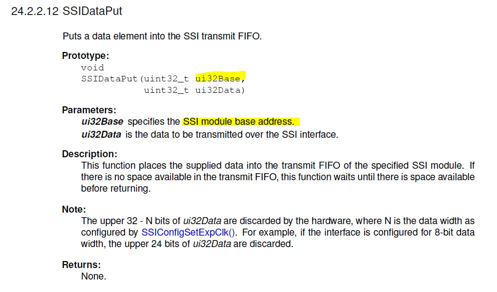
    There is no such API like SSI3DataPut or SSI1DataPut or SSI2DataPut.  The See below API description. 

      I will suggest you try a more simpler example: <TivaWare_Installation>/examples/boards/ek-tm4c1294xl/ssi_master_slave_xfer. This example transfer data between SSI0 (master) and SSI1(slave) one bit at a time instead of in Quad mode. Whether you use ssi_master_slave_xfer or ssi_quad_mode example, please run them as is and make sure they work before modifying them. Another note is that if you change them to SSI3 and SSI2, you need to make sure the interrupt vectors for the new SSI instances are properly updated in the vector table. The vector table is in the startup_ccs.c file. See below example done for SSI1.. If you are going to use SSI2 as the slave you need to setup the ISR vector for SSI2.

    #pragma DATA_SECTION(g_pfnVectors, ".intvecs")
    void (* const g_pfnVectors[])(void) =
    {
    (void (*)(void))((uint32_t)&__STACK_TOP),
    // The initial stack pointer
    ResetISR, // The reset handler
    NmiSR, // The NMI handler
    FaultISR, // The hard fault handler
    IntDefaultHandler, // The MPU fault handler
    IntDefaultHandler, // The bus fault handler
    IntDefaultHandler, // The usage fault handler
    0, // Reserved
    0, // Reserved
    0, // Reserved
    0, // Reserved
    IntDefaultHandler, // SVCall handler
    IntDefaultHandler, // Debug monitor handler
    0, // Reserved
    IntDefaultHandler, // The PendSV handler
    IntDefaultHandler, // The SysTick handler
    IntDefaultHandler, // GPIO Port A
    IntDefaultHandler, // GPIO Port B
    IntDefaultHandler, // GPIO Port C
    IntDefaultHandler, // GPIO Port D
    IntDefaultHandler, // GPIO Port E
    IntDefaultHandler, // UART0 Rx and Tx
    IntDefaultHandler, // UART1 Rx and Tx
    IntDefaultHandler, // SSI0 Rx and Tx
    IntDefaultHandler, // I2C0 Master and Slave
    IntDefaultHandler, // PWM Fault
    IntDefaultHandler, // PWM Generator 0
    IntDefaultHandler, // PWM Generator 1
    IntDefaultHandler, // PWM Generator 2
    IntDefaultHandler, // Quadrature Encoder 0
    IntDefaultHandler, // ADC Sequence 0
    IntDefaultHandler, // ADC Sequence 1
    IntDefaultHandler, // ADC Sequence 2
    IntDefaultHandler, // ADC Sequence 3
    IntDefaultHandler, // Watchdog timer
    IntDefaultHandler, // Timer 0 subtimer A
    IntDefaultHandler, // Timer 0 subtimer B
    IntDefaultHandler, // Timer 1 subtimer A
    IntDefaultHandler, // Timer 1 subtimer B
    IntDefaultHandler, // Timer 2 subtimer A
    IntDefaultHandler, // Timer 2 subtimer B
    IntDefaultHandler, // Analog Comparator 0
    IntDefaultHandler, // Analog Comparator 1
    IntDefaultHandler, // Analog Comparator 2
    IntDefaultHandler, // System Control (PLL, OSC, BO)
    IntDefaultHandler, // FLASH Control
    IntDefaultHandler, // GPIO Port F
    IntDefaultHandler, // GPIO Port G
    IntDefaultHandler, // GPIO Port H
    IntDefaultHandler, // UART2 Rx and Tx
    SSI1IntHandler, // SSI1 Rx and Tx
    IntDefaultHandler, // Timer 3 subtimer A
    IntDefaultHandler, // Timer 3 subtimer B
    IntDefaultHandler, // I2C1 Master and Slave
    IntDefaultHandler, // CAN0
    IntDefaultHandler, // CAN1

  • Hi Charles

    I have done run the project <TivaWare_Installation>/examples/boards/ek-tm4c1294xl/ssi_master_slave_xfer. 

    I Notice the same stuff, there is no clock and Data on the scope.

    Variables are getting updated as below and UART Console is getting with below

    SSI Master-Slave Transfer Example.
    Mode: Legacy SPI
    Data: 8-bit

    SSI0 Sent:
    'T' 'I' 'V' 'A'
    SSI1 Sent:
    'Q' 'S' 'S' 'I'

     Screen Shot of the Same in debug is as below with code stuck at

        while (g_breceiveFlag == 0);  & pui32DataTx[4] gets updated with ASCI Value of TIVA

  • Hi,

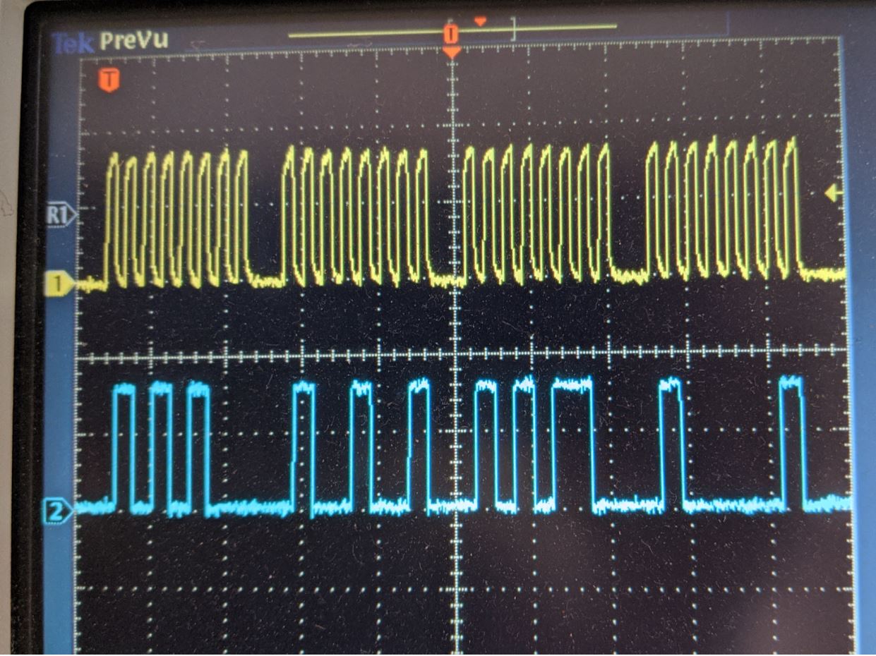
      What board are you using. I just run the example as is, not modifying anything. I probe the PA2 (SSI0CLK) and PA4 (SSI0TX) and I don't see any issue. See below. Do you have another board that you can try?

  • Charles

    We could interface SPI with Flow sensor in non blocking mode. Trying out FIFO interrupt with status check and return immediately