This thread has been locked.

If you have a related question, please click the "Ask a related question" button in the top right corner. The newly created question will be automatically linked to this question.

TIDA-01525: Max Current Limit in the current mirror

Part Number: TIDA-01525
Other Parts Discussed in Thread: OPA2376, OPA2189, OPA2192, CSD22206W, CSD23285F5

Hi team,


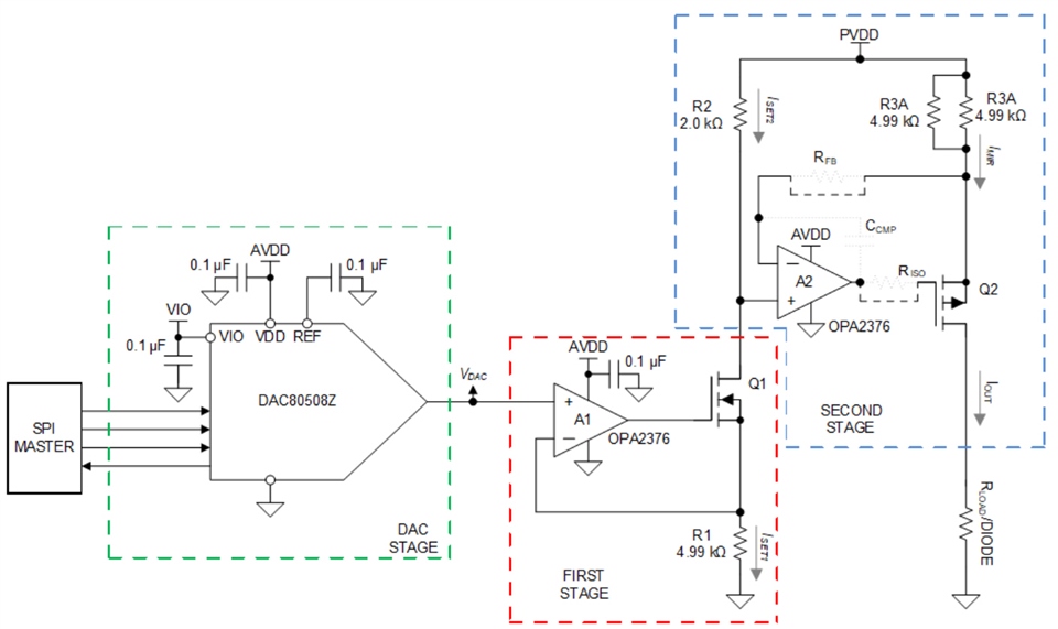
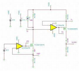
The figure is the voltage controlled current mirror circuit diagram of TIDA-01525.

I want to configure Rload be about 3.5V LED within 1~15A (wannabe 1~20A) contant current.

PVDD, AVDD, max of VDAC is 5V.

1. Assuming that the power of Q2 and R3 is sufficient, is there a limit to the maximum IOUT and Watt that can be applied?

(or limited by the amplification ratio of Iset2 and Imir)

2. If possible, what are the main considerations in this configuration?

3. Can you suggest a design for this?

Thank you.

Hoo

  • Hi Hoo,

    IOUT will be limited by the headroom provided by PVDD. There's a voltage drop across RLOAD, R3, and Q2. You said the LED is 3.5V, so that only leaves 1.5V for the drop across R3 and Q2. If the current is 20A, R3 will need to be very small (in the mΩ range). You'll also need to lower VDAC. I attached a simulation that you can use to test different values. Raising AVDD and PVDD will mean you can have a higher R3.

     TIDA-01525_e2e_20A.TSC

    Best,

    Katlynne Jones

  • Hi Katlynne,

    Thanks for your simulation.

    1. An increase in the value of R3 means an increase in R3 power, so it is being carefully considered. Also, an increase in PVDD means an increase in AVDD, which requires a high voltage on the OPA. (in the current circuit, OPA2376 is 5.5V) I have OPA2189 and OPA2192. (VS 24V)
    Are there any additional considerations and corrections when replacing one of these two?

    2. What are the practical reasons the VDAC should be lowered?

    Hoo

  • Hi Hoo,

    1. This section of the reference design goes over some of the errors in this system:

    You'll want to pick an rail-to-rail op amp with a bias current that is much lower than the reference current (the current through R1). The offset error of the amplifier will also contribute to an offset on the output, so this should be minimized as well. 

    2. Please see the simulation below. You'll see that the output current will saturate with a VDAC of above 1.5V in the example simulation I shared before. 

    VSET will not be able to reach 5V with a AVDD and PVDD of 5V. This would leave no headroom across R2, so you can see the VSET eventually stops increasing and the Vout of A1 saturates at its AVDD of 5V. This happens at a VDAC of 3.75V in my example. 

    In my example, the Vout of A2 also ends up saturating before A1. The drop of R3, Q2, and Rload reached 5V at a VDAC of 1.5V.

    One of these two cases will be the limiting factor of the design. 

    Best,

    Katlynne 

  • Hi Katlynne,

    Thanks for your reply.

    your simulation is very helpful to me.

    1. It is a basically question,

    A1's IN- and OUT are respectively connected to Q1's Gate and Source. 

    Simply thinking myself, there is an insulating layer between the gate and the channel of the MOSFET, so I thought that A1 would be in an open loop state.

    However, the actual circuit passes through the gate and source of Q1 to form a closed loop (negative feedback).

    I understand that this is due to the presence of IGSS (Gate-to-Source Leakage Current) at the Gate and Source of Q1.

    Is my understanding correct?

    2. When considering modifications for my goals, I don't think Q1's choice is very important.

        However, the actual mirrored high current flowing Q2 looks like a lot to consider.

        When selecting Q2, what are the main specifications to check?

        If there is a suitable TI product, it would be better to suggest it.

    3. I want to use 5m ohm 1% 100W for R3. Are there any problems that very small R3 values can cause?

    Thank you.

    Hoo

  • Hi Hoo,

    Your image didn't come through. Can you please try attaching it again? You can drag the file directly into the text box, or select the image/video/file option from the insert dropdown below. 

    The output of the op amp will drive the gate voltage to increase the drain current so that the resulting source voltage (connected to IN-) will be equal to the VDAC voltage on IN+. The loop is considered closed because of this relationship. You are also correct that there is also gate to source leakage current present. When the source voltage can no longer increase due to the headroom issues I mentioned earlier, A1's output will go to it's positive rail as it tries to continue to increase the drain current. In this case, the loop is broken because VDAC/IN+ continues to increase but IN- cannot increase anymore. 

    A lower RDS(on) of Q2 would require less headroom and a larger VDAC voltage could be used before the output current saturates. The simulations uses the same CSD23285F5 from TIDA-01525 which has an RDS(on) of 29mΩ. The CSD22206W from TI has a 4.7mΩ RDS(on).

    I am not an expert in this area, but make sure you have a good PCB layout to avoid trace resistance that could end up adding error to the small 5mΩ R3. Follow any manufacturer recommendations for the resistor you choose. 

    Best,

    Katlynne Jones

  • Hi Katlynne,

    above my Image was captured from the text of TIDA-01525, but you have already given enough answers, so don't worry about it.

    I have already found some conditions that apply your simulation. I will purchase parts for testing. Afterwards, if there are additional questions in my tests,

    would it be better to ask additional questions in this thread?

    Hoo

  • Hi Hoo,

    You can ask additional questions in this thread. I think the thread will lock after 30 days of inactivity, so if that happens then you can use the yellow ask a related question button to start a new thread and we can continue the discussion.

    Best,

    Katlynne Jones