This thread has been locked.

If you have a related question, please click the "Ask a related question" button in the top right corner. The newly created question will be automatically linked to this question.

TIDA-010054: Bottom MOSFET of single leg on secondary side failing

Part Number: TIDA-010054
Other Parts Discussed in Thread: TMS320F280025C, UCC21530

Hi all,

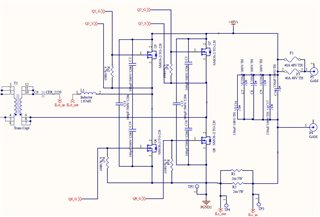
We are working on a 1kW Dual-Active Bridge Converter. During closed-loop single phase shift voltage control, the lower side MOSFET of the first leg on the secondary side is getting damaged (Drain to Source short). On analyzing, we observed overcurrent trip in our trip-zone protection settings. This failure usually occurs during transient variation in load. Deadband provided is 400ns and is sufficient after viewing the Gate to Source waveforms. Can you give us a solution to this problem? Attaching the schematics below. MOSFET Q6 is failing.  

  • Hi Pranav,

    Thanks for reaching out. I am not familiar with this problem, so I need a little more information:

    • Are you using a modified version of the C2000 firmware of TIDA-010054?
    • Which MOSFET are you using?
    • Is L1 the only leakage inductor used, or is there another inductor on the primary side?
    • What is the the Primary side voltage and what is the turns ratio of T1?
    • What switching frequency is used in this design?

    Regarding the Gate Driver circuit I cannot comment, since this is not a TI part and I am not familiar with it.
    I can suggest a TI part as replacement, where we can offer guidance on design.

    Best regards,
    Andreas

  • Hi Andreas,

    1) We are using our own firmware which is loosely based upon the C2000 firmware of TIDA-010054. We are using TMS320F280025C microcontroller for this application.

    2) We are using a Si MOSFET from Infineon with the following part number: IPP030N10N3G.

    3) L1 is the only leakage inductor used. There is no primary leakage inductor. Its value is 2.2uH. This inductor is working well for us and is functioning as expected.

    4) Rated primary side voltage is 400V and turns ratio is 28:5.

    5) Switching frequency is 100kHz.

    The gate driver is very similar to the one used in TIDA-010054. Infineon has made a pin to pin replacement IC for UCC21530.

  • Hi Pranav,

    Thanks for the feedback.

    My first idea is that Q6 might get damaged due to high currents during transient events. Did you check the current of Q6 by measurement?
    During transient events it can happen that the control loop applies the full phase shift, which can lead to temporary high currents. 
    If this is the case the maximum phase shift can be limited, which limits the currents.

    Another note I have, is that the ideal turns ratio is equal to the voltage ratio so N1/N2 = V1/V2. From your schematic I assume that the output voltage is 48V, which would lead to N1/N2 = 8.333. In this conduction the ZVS range is maximized. With this increased turns ratio, the leakage inductance itself could also be increased, which limits the maximum current again.

    Best regards,

    Andreas