A related question is a question created from another question. When the related question is created, it will be automatically linked to the original question.
If you have a related question, please click the "Ask a related question" button in the top right corner. The newly created question will be automatically linked to this question.
Under the designed operating conditions, there can be a large voltage seen at VS. The schottky/zener is a clamping circuit so that VS does not exceed it's abs max rating and damage the device. I recommend you keep this on your design as PMP22288 is proven solution. Thanks!
I believe you mean the Schottky/Zener clamping circuit is limiting the Vs pin current level to 1.2mA.
I understand the necessity. the power supply is designed to operate till 550V. But, I don't think the circuit will help limit the current. That's why I posted the question.
Let me show the calculation.
Doing the calculation at 550V=>
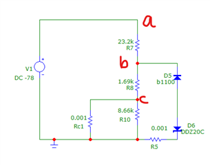
When Q1 is ON, Voltage at Aux-Tp4 = 550V/7 (turns ratio)= 78V ( It would be a negative voltage. but I am not bothered about polarity. I am focusing on current)
When Q1 is ON, Vs pin is pulled to GND by a MOSFET. You can see the block diagram on page 9 of the datasheet.
If I try the see the Aux circuits as active voltage loops when Q1 is ON, I can get two KVLs
1. Aux-R7-R8-internal_mosfet-TP4
2. Aux-R7-D5-D6-TP4
we know that Current takes the least impedance path. and Loop 1 has the least impedance. (if you think Zener will clamp and loop 2 will dominate, please explain)
Current through VS pin or Current through internal MOSFET=> 78V/ (23.2k+1.69k) = 3mA.
I believe it exceeds the Vs pin abs rating and the design is faulty.
The VS pin has a clamp on it of around -250 mV (Vc) . You will need to double check the data sheet for the exact clamp voltage.
When VS goes negative the voltage across R8 max is -Vc-VD4-VD5 = -0.25V-20V-0.3V = -19.95V. The max current through resistor R8 should be 19.95V/R8 = 19.95V/1.69k = 1.18 mA. This current will be the max current than come out of the VS pin. This current is what you are trying to clamp.
If the aux winding does go 78 V below ground, the current through R7 will be 78V-19.95V/R7 = 58V/23.2k = 2.5mA. So based on Kirkoff's current law 1.18 mA will come out of the VS pin and go through R8 and 2.5 mA - 1.18 mA = 1.32 mA will go through D5 and D6. This should prevent the VS pin from seeing more than 1.2mA roughly when the aux winding is negative.
If this resolves your issue, please select resolved at the end of the thread.
When VS goes negative the voltage across R8 max is -Vc-VD4-VD5 = -0.25V-20V-0.3V = -19.95V. The max current through resistor R8 should be 19.95V/R8 = 19.95V/1.69k = 1.18 mA. This current will be the max current than come out of the VS pin. This current is what you are trying to clamp.
Why do you assume Zener would be in Breakdown? You can take Vd6 as 20V if and only when Zener is under breakdown.
Vs pin is across R10. When Q1 is ON, Vs pin is pulled to GND by an internal MOSFET. So, I added a 1mohm resistor across R10. Ultimately, Vs pin current or Current through Rc1 need to be found.
Since R10>>Rc1 , Current through R10=0mA
So, Current through Rc1= Current through R8.
Finding current through R8
1. Disconnect D5 and D6 for calculation purpose.. Now,it becomes a simple voltage divider.
V1= -78V
V(R8) = V1 x R8/(R8+R7) = 5.3V ( This is the voltage between Node b to ground)
I(R8)=3.13 mA
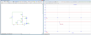
Below is my simulation graph.
My reason for Zener not undergoing breakdown is that the Voltage between node B and gnd is only 5.3V.
An important condition for Zener breakdown is that the Input voltage to Zener must be greater than Vz of Zener.
You have the VS pin as an open. When the aux winding is negative there is a 250 mV clamp across the low side VS resistor to ground.
The current coming out of the VS pin when the aux is negative (IVS) = (VD6+VD5-250mW)/R8
IVS = (0.6V + 20V - 0.25V)/1.69k ohm = 12 mA.
Now that I have studied this again R8 is too small. It should be at least a factor of 10 times greater than this. You are correct that an R8 of 1.69k is too small to protect against an over current.
I would make R8 > or = to 20.3V/1mA = 20 k ohm. Then adjust R7 to control the output voltage. Then you should be O.K.
In this case if you swap R7 and R8 that could work. This will maintain the VS divider ratio to control the output voltage.


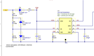 Can someone please explain the purpose of D5 and D6 in the Auxiliary section? Thanks in advance