This thread has been locked.

If you have a related question, please click the "Ask a related question" button in the top right corner. The newly created question will be automatically linked to this question.

TIDA-050047: Schematic Review of Customized Design based on Ref Design with Dual Power and LM61495

Part Number: TIDA-050047
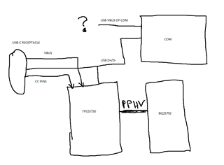
Other Parts Discussed in Thread: TPS25750, USB2ANY, BQ25792

Hello!

I am a beginner with electronics design after about 12 years my electronics engineering degree. 

Could anyone be helpful to review my schematic attached as pdf?

Best Regards.PowerSupplyV0.8.pdf

  • Hi Hassan,

    I will review schematic and provide feedback no later than Monday February 13, 2023. Thank you for your patience!

    Very Respectfully,

    Brandon Beader

  • Hi Hassan,

    For a beginner you did very good! I have review your PD portion (TPS25750) and have the following feedback:

    • You have setup for the PD to be flashed via I2C2ANY, however this is not what we recommend for flashing device. Using I2C2ANY you will have to write your own flash sequence to comply with our PD. We recommend using ARDVARK adapter instead.
    • You ADCIN decoded values correlate to the following, make sure this is what you want. 
      • Dead Battery Mode: AlwaysEnableSink
      • 7Bit Slave Address: 0x21
    • Using D+/D- for BC1.2 support. Make sure to enable in your configuration.

    I have attached excel file we use for review that has my above comments filled in!

    Very Respectfully,

    Brandon Beader

    Schematic Checklist Rev 0p3.xlsx

  • Thanks a lot Brandon. I really appreciate it. 


    Having a permanent ARDVARK header on the board raises physical constraints. Are there any alternatives with a smaller footprint? Maybe have a smaller header and make an adapter for it? 

    Either way, Thanks again!

    Best Regards,

    Hassan. 

  • Hi Hassan,

    How do you intend to flash your EEPROM? I am looking again at your schematic and I see no connection to EEPROM from external connector in order to flash EEPROM. The slave I2C lines on the PD are mostly used either for debug or MCU to read/write into device as necessary. Your patch bundle and configuration should be loaded into the EEPROM which will be loaded by the PD during bootup from the I2C master lines.

    As for the Ardvark connector, I would recommend making an adapter or using an MCU to flash EEPROM via Micro or Type C adapter. Typically, our customers will confirm their firmware works as intended and burn in the EEPROM in order to remove Ardvark header or flash connector.

    Very Respectfully,

    Brandon Beader

  • Hello Brandon. Thank you for the comments. 

    I had intended to use the I2C slave from a computer on module present on another sheet. My program was to turn on the device using battery power in default configuration and use the i2c slave lines to program the device and write to flash at startup. In order to not need any external flashing. The usb2any was kept as a backup at the moment. 

    The datasheet mentioned somewhere that if no configuration is present in eeprom, the device will boot up using default parameters. 

    Kindly advise if I did not get it right. 

    Best regards,

    Hassan Hafeez. 

  • Hi Hassan,

    You are correct, the PD will boot up with the default configuration that is set using ADCINx values.That is okay, just wanted to make sure!

    Very Respectfully,

    Brandon Beader

  • Hello Brandon, 

    I have a follow up question regarding using D+/D- for BC 1.2 support. 

    Do the D+ and D- go to both TPS25750 and BQ25792? or just TSP25750 and it can control the BQ25792 using I2C master? 

    Can I use these signals for USB2 Data at the same time? if so, how would I lay them out on PCB? fork them from the connector or from the nearest IC (TPS or BQ)?

    Best Regards,

    Hassan Hafeez. 

  • Hi Hassan,

    You can not connect the D+/D- to both PD and BQ device, this will cause issues. Is there a reason you need BC1.2 support?

    Yes, you can use these lines for USB2 data. Please see below diagram for startup sequence for BC1.2 on D+D- lines. 

    Very Respectfully,

    Brandon Beader

  • Hello Brandon,

    Thank you for the diagram. I want to support BC1.2 in order for the proposed device to be able to charge from a variety of chargers on the market. I do not intend to create a charger product for my device. 

    Thanks again!

    Best Regards,

    Hassan Hafeez. 

  • Hi Hassan,

    I see and that makes sense!

    Currently TPS25750 GUI does not have BC1.2 support. This feature will be added in the next FW release which can be expected in the next couple weeks!

    Very Respectfully,

    Brandon Beader

  • Hello Brandon!

    Sorry to bother you again regarding this. But I am trying to achieve a UFP mode device with the TPS25750 so I do not have to add another usb port to the device. Is it possible in this scenario? The internal COM (Computer on Module) has a 5V max voltage on VBUS. If I use the VBUS from PD port directly, it would harm the COM. Do you have any suggestions regarding this such as maybe use a comparator? or a data role capable pd chip? or maybe a mux to work with the tps25750?

    Upon further investigation, in the reference design, PP5V is used to source 3.3V. Can I use this PP5V as VBUS for the COM? 

    Also, there is a GPIO Event as follows which may be able to be used to drive a standby 5V supply as vbus through a mosfet?

  • Hi Hassan,

    Do you have a block diagram for what you are trying to achieve? From your question above I am assuming you intend to use this port for sink/UFP, is this correct? This will help me better understand what you are trying to achieve and how it can be supported!

    Regards,

    Brandon

  • You are correct! I am trying to achieve sink/UFP on the same port. If PD detects a normal usb connection (without PD/charging capability), I want the COM's usb connections to be enabled. A very crude block diagram is as follows:

  • Hi Hassan,

    That block diagram is sufficient! You are able to set PD as UFP/SINK if BC1.2 is not needed. Even if BC1.2 is needed, you can still support UFP however based on your block diagram you want to disabled COM.

    Therefore, there are some options in which you can do. You can use an LDO off of PPHV in order to generate your USB VBUS and have this enabled/disabled using GPIO depending on if device is a sink or source. So for your case you will disabled LDO if acting as source! I would also not recommend attaching anything to VBUS on the Type-C port. 

    Regards,

    Brandon 

  • Thanks a lot, Brandon. I have one more request. Kindly also suggest an LDO to work with VBUS when VBUS of Type C is at 5v. I have been trying to find an LDO with low dropout voltage. But I was only able to find at least 2V dropout. Would 3V be enough for COM's VBUS to recognize device attachment?

  • Hi Hassan,

    The LDO would need to be on the system side of the PD. Attaching an LDO to VBUS directly will cause you to fail compliance therefore I recommend you add this LDO to PPHV. 

    The LDO's that I am very familiary with are TLV755xx family and are pretty straight forward devices.

    Regards,

    Brandon

  • Hi Brandon!

    Thank you for the suggestion. Yes, I added it to the PPHV as you earlier suggested. I was just wondering if VBUS is at 5V, then PPHV would also be at 5V. The Output of the LDO would then be less than 5V Maybe around 4.5V. I added TLV70245QDSERQ1 with fixed 4.5V output to remain compliant with the VBUS range of COM.