This thread has been locked.

If you have a related question, please click the "Ask a related question" button in the top right corner. The newly created question will be automatically linked to this question.

TIDA-010054: ZVS range graph plot query

Part Number: TIDA-010054

Hello,

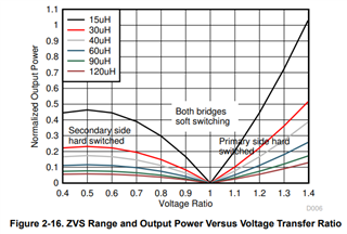
For the dual active bridge topology at Bidirectional, Dual Active Bridge Reference Des for Level 3 EV Charging Stations (Rev. C)., we have query for plotting the graph below -

We are working on 7kW onboard charger design.

Can you please let us know how to plot this graph.

For X-axis, Voltage ratio = (Vout / Vin) * N; where N = turn ratio (Np / Ns).

Have you used any equation, formulae to plot this graph?

The motive behind this is to find the ZVS region for DAB topology. Or pls suggest how to find the ZVS region graphically.

Regards,

Abhishek D.

  • Hi Abhishek,

    These graphs are plotted based on ideal equations for current and voltage waveforms explained in Figure 2-15 of the design guide.

    For zero voltage switching the inductor current needs to change sign before the switch event, in order to make the body diode of the switches conductive before the actual switching event.

    The current waveform can be calculated by  U = L* di/dt as a piecewise-linear function with the applied voltages, the selected phase shift and the selected inductance.

    Here the equations for i1 and i2, based on Vp, Vs, L, the switching frequency fsw and the phase shift phi:

    with V2 = d*V1/N. (see equation 9) Please note that n = 1/N, I will use small n,  which is Primary Turns/ Secondary Turns for the upcoming equations

    First we need to calculate the length of interval 1 and interval 2:

    T1 = phi/(2pi) * 1/ fsw

    T2 = 1/(2*fsw)

    Then we can calculate the current IL at t=0

    i0 = - (T1*(Vp+n*Vs)+(T2-T1)*(Vp-n*Vs))/(2*L);

    i1 = IL0 + (T1*(V1+n*V2)/L);

    i2 = -i0


    With the conditions i1 > 0 for soft switching of secondary side and i2 > for primary side soft switching, we can set i1 = 0 and i2 = 0 and solve for phi (phi is part of T1 and T2) in order to find the ZVS boundary. This is true for ideal switches, ideal diodes and no output capacitance of the switching devices.

    If we solve these with Matlab we get:

    Primary side ZVS boundary: 
    phi  = -(pi - pi*d)/(2*d)

    and secondary side ZVS boundary:
    phi = pi/2 - (pi*d)/2

    Now we can do a swipe across the voltage ratio d from 0.5 to 1.5 and will get a ZVS boundary based on the phase shift phi.
    The phase shift can be converted into the power by equation 6:

    Now you can plot P over d and will get a curve like this shown in Figure 2-16. 

    Best regards,

    Andreas