Part Number: PMP8740
Other Parts Discussed in Thread: UCC28950
Introduction
We are currently engaged in the development of a charger design involving a set of three distinct printed circuit boards (PCBs). Two of these boards have been designed successfully and are functioning as per expectations. The remaining third board, however, is presenting some challenges, particularly in its integration with a Phase Shift Full-Wave Bridge (PSFB) rectifier.
Design Layout
Figures 1 through 4, included in the report, provide a comprehensive understanding of our design. Figure 1 outlines the complete schematic of the charger design. The simplified schematic of the PSFB rectifier, a significant component of our design, is depicted in Figure 3. Figure 2 focuses on the MOSFETs driver circuit, while Figure 4 provides a detailed view of the MOSFETs along with the inductor and transformer on the primary side of the circuit.
Issue Description
Our primary issue stems from irregularities observed in the waveform behavior at the gate pin of the MOSFETs. Under conditions where no voltage is applied to the H-bridge, the MOSFETs exhibit an ideal and clean waveform, as shown in Figure 5. However, applying voltage to the H-bridge introduces negative spikes on the gate pin during the MOSFETs' turn-on phase as shown in Figure 6. The intensity of these spikes tends to escalate with an increase in the applied voltage. Subsequently, this phenomenon is leading to damage to our MOSFET driver Integrated Circuits (ICs).
Attempts at Resolution
In an attempt to diagnose the cause of these negative spikes, we have analyzed equivalent circuits to scrutinize the gate driving IC loop path. Interestingly, all these circuits seem to corroborate the occurrence of negative spikes during the MOSFETs' turn-off phase, an anomaly which is efficiently managed by our driver IC. However, the theoretical basis for the emergence of these spikes during the MOSFETs' turn-on phase remains elusive.
Conclusion
At this stage, we are actively seeking an effective solution to address the root cause of the negative spikes during the MOSFETs' turn-on phase. Any insights and suggestions on how to prevent these spikes from causing damage to our MOSFET driver ICs would be greatly beneficial to our ongoing development process.
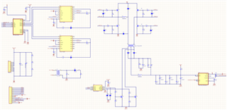
Fig.1 Schematics of PSFB rectifier
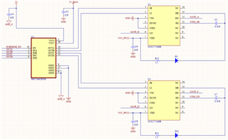
Fig. 2 Clear picture of MOSFET driver for Transformer primary side MOSFETs
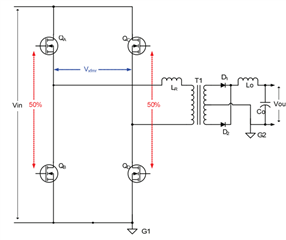
Fig 3. A Phase-Shifted Full Bridge Circuit simplified schematics
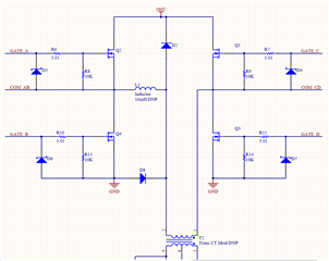
Fig.4 Clear picture of Primary side MOSFETs circuit
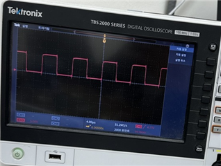
Fig. 5 Waveform of PWM signal on Gate of MOSFET without giving drain voltage
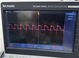
Fig. 6 Waveform of PWM signal on Gate of MOSFET with 12v drain voltage