This thread has been locked.

If you have a related question, please click the "Ask a related question" button in the top right corner. The newly created question will be automatically linked to this question.

TIDA-00178: Interface to a Sin/Cos Encoder Reference Design

Part Number: TIDA-00178
Other Parts Discussed in Thread: THS4531, , ADS8354, THS4531A

Hi Team, 

Good day. I am posting this inquiry on behalf of the customer.

I would like to take over the reference design TIDA-00178 for a project.  In the example project, a gain factor of 5 is set for the THS4531.
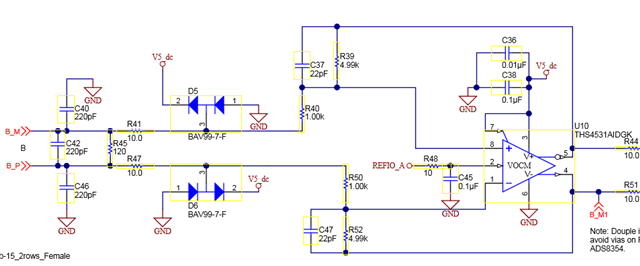
As a power supply, the chip has 5 V. If I amplify 1Vpp by 5, then I have between 0 and 5V.  The output voltages do not go up to 5 V, but rather 4.9 V.  

If my 5V power supply fluctuates by 5%, it gets even less.

So with a gain of 5, I will have problems in the 0V and 5V limits. 

The signal is cut off above and below.

What am I missing here?  I'd love it if you could help me.  

Thank you for extending your support. Your help is much appreciated.

Kind regards, 

Marvin

  • Dear Marvin,

    thank you for sharing your customer's question.

    We have differential input and output signals. The differential input signal is specified from 0.6Vpp to 1.2Vpp. Note this is peak to peak. For a 1Vpp signal, we get two differential signals which each only have 0.25V amplitude. Now if we subtract the differential voltages we get +0.5V as peak positive differential voltage and -0.5V as peak negative differential differential voltage. Now the peak to peak voltage is 1Vpp. Please check the output specifications of Sin/Cos encoders listed in the design guide. 

    The data converter has a differential full-scale input range of +/- 5V, hence 10Vpp. That means with again of 5, we are only using 50% of the ADC full scale range and
    avoid to get close to GND and close to 5V rails.

    Please note we assume a 2.5V common mode voltage of these differential voltages. 

    Sticking with 1Vpp differential input, and corresponding 0.25V amplitude per each differential signal we get +/-1.25V at a gain of 5. Adding the 2.5V offset, the ADC will see 1.25V to 3.75V range for each of the two differential signals equal to 5Vpp.

    So we have 50% headroom and allow therefore 1.2Vpp inputs and wil be far from 0V and 5V rails. 

    For more info, please refer to the Design guide — TIDA-00178 section  4.1.1.3 Differential Amplifier THS4531A and 16-Bit ADC ADS8354

    Please let me know when you have additional questions. 

    Thank you.

    Regards,
    Martin Staebler