This thread has been locked.

If you have a related question, please click the "Ask a related question" button in the top right corner. The newly created question will be automatically linked to this question.

PMP11371: Layout UCC28740 - CS pin layout

Part Number: PMP11371
Other Parts Discussed in Thread: UCC28740

Dear TI,

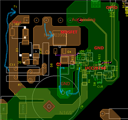
may anyone look at below layout,cricital area are marked with correspondding text, the area shown is around 65mm vertical x 60mm ,

my concern is CS pin routing and placement, 

i tried to route UCC28740 GND and CS PIN return path through separate traces, the trace between  CS resistor and Bulk cap is  around 10mm long, 

pls give your comments , below is snapshot of placement, routing , 

let know if i am clear, if more information is needed 

 Post

Regards

ls

  • Hi ls,

    This configuration will add parasitic inductance to both the CS path and DRV path. I would add a GND connection by where R22 and R19 are to reduce the inductance for those connections. For the connection you can use a thinner trace to separate the power and signal loops, the higher current from the primary loop would follow the wider trace you have now and the signal lops will flow through the other connection that has less inductance.

    Let me know if you have any questions on this.

    Thanks,

    John

  • Hi John,

    thank you for looking and providing suggestion ,

    now keeping a thinner trace for CS and DRV loop on pcb, and power path remains as it is through a wider trace 

    Regards

    Ls