A related question is a question created from another question. When the related question is created, it will be automatically linked to the original question.
If you have a related question, please click the "Ask a related question" button in the top right corner. The newly created question will be automatically linked to this question.
Are you using the same output capacitors and coupled inductor as in PMP10081. If not, it is very likely that you will need to adjust the compensation components to get a stable system.
The output capacitance selection depends on your application requirements. If you expect to have load transients it's better to work with the equations from the TPS40210 datasheet as it provides some more margin (or you use a more precise impedance based calculation method like here: https://www.ti.com/document-viewer/lit/html/SSZTCQ4). If you only care about ripple, then take the equation from the app note.
Hi Nithin, there are two loops that are competing with each other. The current is sensed by R14 and has some gain stage from U2A circuit that can be adjusted by R17 to create a voltage (CS) that gets divided down to the FB. This means the controller will at first regulate the current to the FB voltage. Eventually the batter will get charged up to a certain voltage in set by the voltage loop (R18/R19). Then D5 turns OFF, D4 turns ON, and the converter jumps to voltage regulation of 13.8V
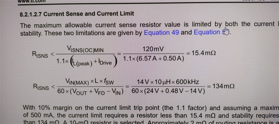
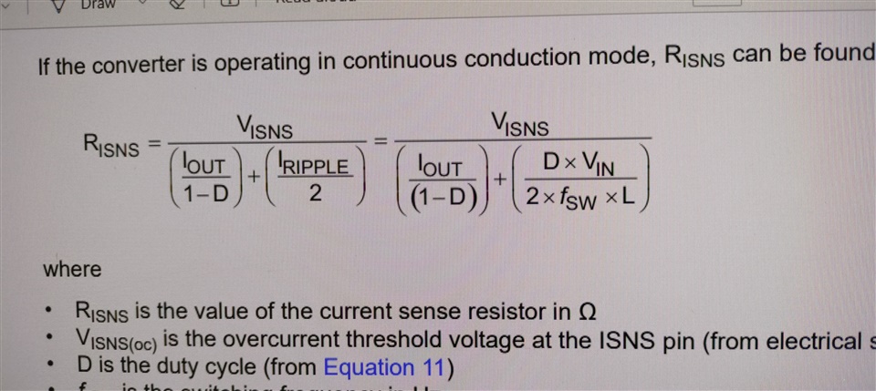
To calculate the sense resistance you just calculate your peak current through the MOSFET and add some margin. You can use a tool like TI Power Stage Designer (www.ti.com/powerstage-designer) to do this.
The second equation you posted is for a boost converter, so it won't fit for a SEPIC design. You can look up equations from the Power Topologies Handbook (https://www.ti.com/seclit/ug/slyu036/slyu036.pdf), too.
If your maximum peak current (including efficiency) is 3A, you should still allow some margin for load transients and temperature effects, e.g. 30% more. The equation you are using is correct, but you also need to check the conditions when VOCP is 120mV or 180mV.
The Power Stage Designer Tool does not support the SEPIC topology in the Loop Calculator as the SEPIC transfer function is quite complex.
In general, you can only go for 1/10 of the switching frequency, if your error amplifier allows such a high bandwidth (1/100 of the GBWP is reasonable) AND if it is a buck derived topology.
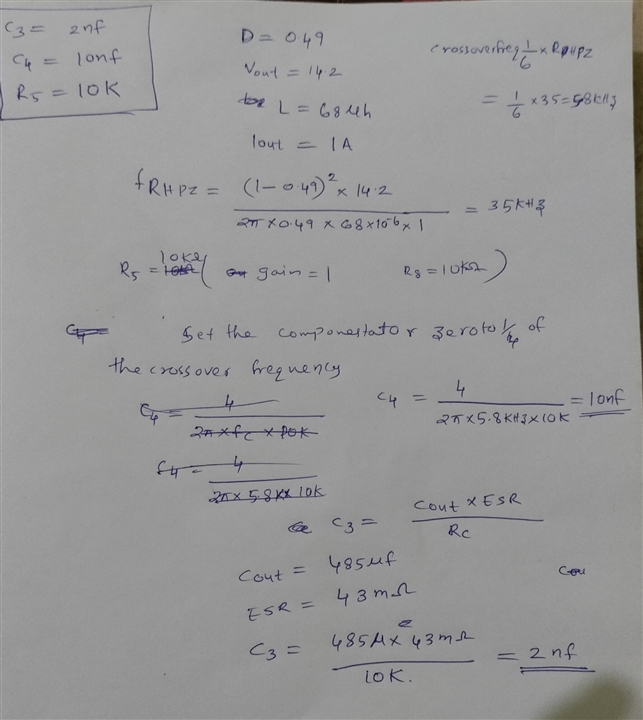
If it is a boost/buck-boost derived topology (e.g. Flyback, SEPIC), you have to consider the right half plane zero (RHPZ) and then the maximum achievable crossover frequency is 1/5 to 1/10 of the RHPZ frequency.
For these more complex topologies it is good practice to start with a conservative compensation network and then optimize it in the lab by using a network analyzer.
For a battery charger you don't really need a high bandwidth in the voltage control loop as there won't be any quick and large changes to be expected.
Good practice is to put the crossover frequency to 1/10th of the RHPZ, the zero to 1/10th of the crossover frequency and the pole on the RHPZ frequency. With that you have the full phase boost of the zero at fco and the pole will only start to reduce the phase slightly above fco. For your case that would mean having the zero at 350Hz, fco at 3.5kHz and the pole at 35kHz. Please keep in mind that this recommendation would be for voltage control only, in a charger application it can be beneficial if the voltage loop is slower than the current loop.