Hi
My customer plan to build this PMP22650 following exactly PMP22650's layout file.
We got several question need clarify before using the layout file to build PCB.
- can we use 35um cooper thickness (1 oz. of copper ) for top and bottom layer ? for rest of the layers following the original design 61um cooper thickness (2 oz. of copper)
- For all the φ0.20mm,φ0.25mm via holes, can we fabricated them with resin plugging + POFV (plated over filled vias).
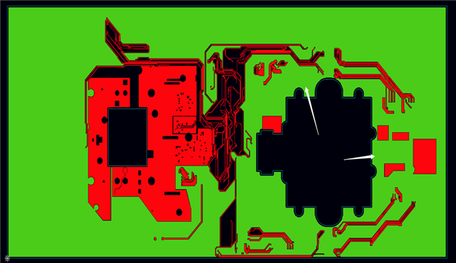
- In the gerber file, indicated as below, It is less than 0.400mm between the non-plated-through-hole(NPTH)and the holes filled with resin .If the Gerber data are followed to do, the resin will flow into the NPTH and get remained on the NPTH wall, resulting in smaller diameter of holes , affecting assembly and orientation at your side . Can we slightly move them apart to achieve 0.400mm distance between them
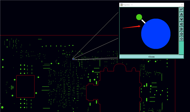
- location indicated below, The opening of the NPTH hole is too large, copper may be exposed on the adjacent conductors. Can we narrow the opening and move the conductor appropriately to avoid exposing copper?
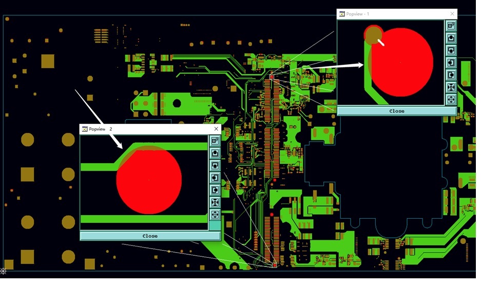
- As below picture shows, the spacing between some NPTHs and the inner-layer line is insufficient. can we slightly move the line to increase the distance between hole and the lines?

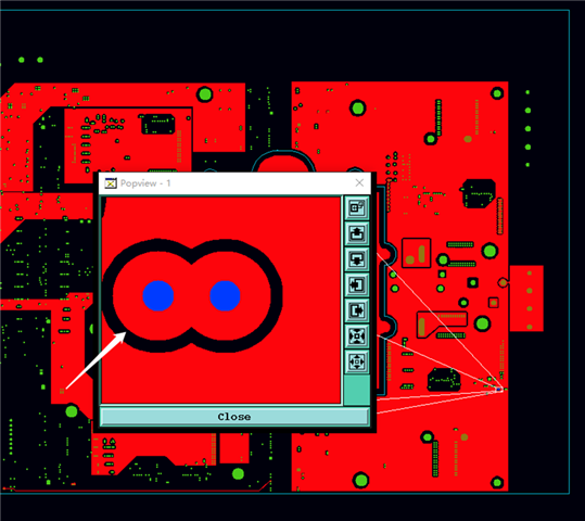
- As below picture shows, the 2 blue holes in the figure are the same network, but only one hole in layer L6 has a PAD.
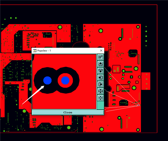
Can we also add PAD to the other hole so that they are connected, this will not affect the network ? to make it as below ?
8. At layer 2 and layer 7, As the copper-free zone of inner layer is very large, then bubble, insufficient flow of glue is prone to occur during lamination, leading to the risk of de-lamination.
Original layout as below
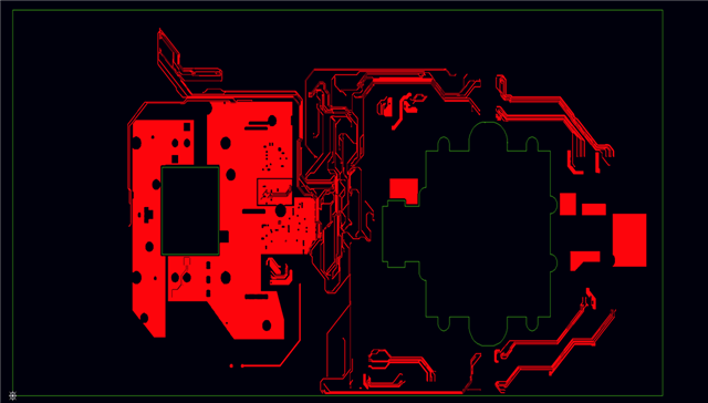
Can we add dummy copper on the layer 2 and layer 7 appropriately as below ? (The added copper is kept away from all the circuits and drill holes .)
