This thread has been locked.

If you have a related question, please click the "Ask a related question" button in the top right corner. The newly created question will be automatically linked to this question.

PMP11303: PMP11303

Part Number: PMP11303
Other Parts Discussed in Thread: UCC29950, , PMP, PMP11237

Hi TI,

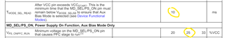
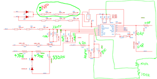
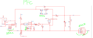
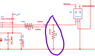
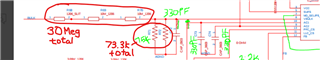
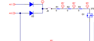
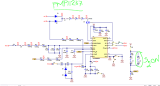
  good day. I'm designing 300W SMPS with UCC29950D (with auxiliary bias mode).  this is my reference from TI PMP11303. as per your recommendation 1st I'm starting with the PFC section. but the PFC-GD not  delivering the PWM. The ucc29950 giving issue. but im giving all those inputs properly. kindly provide us with test methods to check if IC working or not and also any other predefined input values in pins that will provide us with an output, to check if pin functionalities are working properly and also provide us support on generating the PWM output signals.

  • Hello K.Prabhu, 

    Thank you for your question on the UCC29950 PFC operation.  I'll try to help you obtain PWM at the PFC-GD pin.

    I believe that it was your intention to provide all inputs properly, but simply saying so is not sufficient since you might have missed one unintentionally.
    It is better to use a specific check-list of the voltage or current and sequence that you provide to each input, to verify that all requirements are met.

    According to the datasheet, for the PFC section to run:

    1.   VCC > 10.5V to start up and stay >10V to run.
            
          For testing, I suggest to use a +12V bias supply with at least 100uF output capacitance and > 200mA current limit. 

    2.  Some level of AC signal at the PFC input so that the current into AC1 or AC2 meets the the turn-on threshold (brown-in). 
         

    3.  Make sure that the MD_SEL/PS_ON pin is held to 0V for at least 10ms before raising it above 33% of VCC. 
         

    4.   Per Figure 21 in the UCC29950 datasheet, allow some time (100~200ms) for PFC_GD pulses to begin. 

    Regards,
    Ulrich

  • Hello TI,

    thanks for ur reply

    auxiliary bias mode.

    i have an attached the UCC29950D IC section and PFC section. kindly review it.

    While turn ON AC,

    slowly increasing the AC 0 to 100VAC.

    auxiliary bias mode.

    Auxiliary power supply voltage VCC=13.2V

    AC-DET pin voltage showing =0.2v (almost 0V)

    MD-SEL/PS-ON pin voltage applied=6.6vdc for PFC section turn on.

    kindly guide me to take off the project.

  • Hi TI.

    Test results.

    1..... VCC=13.2v applied above 10.5v 

    2.....AC threshold current meets as per expectation 9uA(3.27Mega ohm series with AC1 same as AC2 also).

    3.....We applied VCC13.2V first. after that turning on by external switch,. then applying voltage at MD-SE/PS-ON=6.6v (above33% of VCC)

    4..... after that 200ms,PFC-GD pin pulse not coming..

    kindly provide the solution.

  • Hello K.Prabhu,

    Thank you for providing the updated test information and marked-up schematics. 

    Following the connections, I do not see any problem with the schematic diagram.  However, it is low resolution and the text is small and fuzzy.  I can't read the values very well. 

    When you say that PFC-GD pin pulse is not coming, are you probing the PFC-GD pin or probing the gate of the MOSFET Q1? 
    This part from MOSFET gate-to-source looks like 0 ohms (but it is difficult to read). 

    If it really is 0 ohms, then there can be pulses at the PFC-GD pin, but no pulses at the MOSFET gate. 
    Please check this.  

    That brings up another point.  When debugging a prototype board, the board may reveal an error in the schematic, OR, the schematic may be perfectly good but there is a problem on the board itself.  
    If the schematic values and connections are all good, then examine the board for wrong components, backwards diodes, or missing parts. 
    Some subtle problems are the result of short-circuits from solder bridges or from open circuits due to tool damage or a scratch across narrow tracks. 
    A ceramic capacitor may be shorted or low impedance due to cracking from board flex.  
    Please look for such things.  

    Also, if you have not already done so, please try replacing the UCC29950 with another one, in case the existing one became damaged somehow. 

    Regards,
    Ulrich

  • Hi Ulrich,

    thank you for your response. your wright. schematic values wrong. but gate source resistor pull down 10k. pull up 3.3ohms only.

    we tried replacing with new UCC29950D IC. the PFC-GD came while turn on the AC, but after that PFC-GD gone. How to make sure continous work? kindly guide me

  • hi,

     we tried replacing with new UCC29950D IC. the PFC-GD came while turn on the AC, we got output in PFC bulk 480vdc. but after that PFC-GD gone. How to make sure continuous work? kindly guide me

  • Hello K.Brabhu, 

    If you get 480Vdc on the PFC output, it seems to be working open-loop or wrong set point.
    In other words, there is no feedback or wrong feedback from PFC output to the controller. 

    Please make sure these parts are loaded correctly:

    These values will set PFC Vout to = ~386Vdc.

    Regards,
    Ulrich

  • Hi Ulrich,

    Good day.

    I  have clarification. TI was used pq35/35 core &bobbin in LLC section as per refer design PM11303. primary inductance value mentioned 200uH to 220uH. also mentioned 32 Turns primary side . secondary turns 4Turns for 12v output .  but AL value of this core  4uH mentioned in datasheet.

    1....Do we required 32Turns primary for achieving 200uH.? Because for the 200uH inductance (L=ALvalue*N*N) will achieve less turns only. why we need to go 32T?

    2....Is it required the Airgap between the core fore achieving the 200uH? or any other type of material needed? 

    3---This half bridge LLC topology. really required  Airgap between core?

    Im little worried about the LLC transformer primary inductance configuration.  Kindly help me. How to match the 200uH inductance along with 32Turns. 

  • Hello K.Prabhu, 

    A PQ35/35 core is usually made from ferrite material.  A specific AL value of a core-shape set is based on whether it is ungapped or factory-gapped.  
    In my Ferroxcube catalog, several materials in this core shape have ungapped AL values ranging from 4570 to 6000 nH/N^2.  
    I don't know the material used in the PMP11303 LLC transformer design, but 4000nH/N^2 (4uH/N^2) seems reasonable for an ungapped structure. 
    Ungapped, the transformer magnetizing inductance would be 4uH*32*32 = 4096uH.

    Definitely, the PQ35/35 transformer must be gapped to reduce inductance down to ~210uH +/-10uH.  
    All ferrites usually require an air-gap to achieve a targeted inductance value, although the width of the gap may vary from one material to another. 

    The number of turns in the transformer is usually determined by the maximum allowable flux density, not by the AL value.  

    This discussion is deviating into magnetics design theory, which is beyond the scope of this E2E forum.  
    For further information, please search the internet where you can find almost unlimited support on that topic.

    Regards,
    Ulrich

  • Hi Ulrich,

    thanks for your reply. In PMP11303 design, mentioned  some inputs for the LLC transformer.,

    a)......primary inductance 220uH,

    b).......turns ratio=32:4:4.

    c)........also used PQ35/35 core  or  PQ type core

    my question is,

    Im following as per TI input data. i was used PQ35/35 core, turns ratio=32:4:4. but only one thing i want to know. 

    1.....Do we need airgap for the LLC transformer or not. To achieve 220uH inductance value.?

    or do not need airgap?

    kindly guide me.

  • Hello K.Prabhu, 

    I had answered your question in my previous reply: 
    "  Definitely, the PQ35/35 transformer must be gapped to reduce inductance down to ~210uH +/-10uH.  "  (See in middle of reply.)

    This thread is about support for the PFC part of UCC29950 as used in the PMP11303 reference design.  
    If you need further support concerning the LLC part of this design, please start a new, separate thread on LLC control issues so that the appropriate expert can reply to you.  

    It seems like the PFC part is concluded and I will close this thread. 

    Regards,
    Ulrich

  •           


    Issue on TI board: 

    1...AC1,AC2 track are burned, while turn-on .Also D1,D2 diodes are failed. im using PMP11237 (SELFBIAS MODE) design.same PCB layout PCB.UCC29550DR IC. components same, including transformer also. I thing The IC have an issue. 

    I checked another board also. I was removed the D1,D2 diode, the circuit do not have an issue. only when enable D1,D2 diode that time only issue. i means once go for turn on the IC only the issue with IC. plz  help us.


  • Hello K.Prabhu, 

    What kind of MOSFET are you using at Q1 (shown in the snippet above)?  What is its part number? 
    Q1 should be a depletion-mode MOSFET, not an ordinary enhancement-mode MOSFET.

    I am not sure how an enhancement-mode FET will react during start-up, but I suspect that its Gate voltage may exceed its Source voltage by more than 0.3V.
    The Absolute Maximum rating of V_SUFG is V_SUFS+0.3V. 

    One other possible cause of failure is if you are testing with a DC input voltage.   The SUFG/SUFS self-bias mode requires only an AC input because zero-crossings must be detected at SUFS.   A DC input will have no zero-crossings and the UCC29950 will react as if AC had been removed and will start the X-cap discharge process.  With DC input, the X-cap voltage can not be discharged and the IC will keep trying to discharge so at some point one of the devices in the discharge path (either Q1 or the UCC29950) will over heat and fail, leading to the other device failures, too. 

    Please make sure that you are using a depletion-mode MOSFET and only AC input during your testing. 

    Regards,
    Ulrich

  • Hi Ulrich,

    I/p volt= 90VAC  to  260VAC

    selfbias mode PMP11237 pcb layout pcb.  we are assembled as per TI Components.

     Q1= BSS126 H6906 depletion mosfet.

     but UCC29950DR IC did not powered up issues,

    transformer winding ratio 32:2:4:4

    condition 1:

    S2 Switch turn on, 

    Input 230vac ON,

    Results:

    measured voltage at VCC =0.5VDC,

    eventually not getting PWM pulses. so that auxiliary winding not generated VCC.


    NOTE:

    And also, LDO TPS7A1601DGNT IC also externally. with 20v input already verified. The IC are regulating voltage 13vdc.

    The PFC gate driver UCC27511BVR& LLC gate driver UCC27714D IC are verified with external PWM pulses. its driving mosfets properly
     driver IC are working properly.

  • Hello K.Prabhu, 

    Thank you for the additional information. 

    It could be that a previous failure at start-up (due to unknown problem) damaged more parts than you thought. 
    Previously, U1 pin 4 (SUFG) may have been shorted to pin 5 (SUFS) or pin 3 (VCC) by a solder ball or other solder short. 

    Whatever the previous cause, if the Start-Up Fet (Q1) fails as a short-circuit, it will allow high voltage through and will probably damage all parts on the VCC rail, including the VCC filter capacitors.  Any one of them could be holding VCC low to about 0.5V if you did not find all bad parts after the previous failure.  

    I recommend to remove all components connected to VCC and replace them with new parts.
    Make sure the pads are clean and no solder bridges exist after installing the new parts. 

    I also suggest to verify that the new PFC controller starts up by applying a DC bench supply to Q1 drain while keeping AC power off. 
    Start the DC supply at 0V and dial it up by hand high enough so that VCC reaches the start-up threshold. 
    If that works, then remove the DC supply and apply AC input. 

    Regards,
    Ulrich

  • Ulrich,

    Thank you for your reply. 

    I got your point. But don't have an issue with soldering and components. why that depletion mosfet & ucc29950dr IC getting fail? why its suddenly getting fail.?

  • Hello K.Prabhu,

    The UCC29950 will fail after the BSS126 fails, because high voltage becomes applied to the SUFS and SUFG pins.  They are not rated for high voltage. 
    The high-voltage depletion FET is intended to block the rectified AC voltage from the SUFS input.  UCC29950 failure is follow-on damage from depletion FET failure. 

    So the question is what causes the BSS126 to fail?  Well, that FET must be experiencing some kind of overstress that it cannot sustain. 
    It could be overvoltage on Vds due to surge voltages or spikes on the AC line, or maybe excess drain-source current leading to excess TJ rise, or excess Vgs from spikes of some sort.  

    Voltage spikes on the AC line may come from contact-bounce of a relay or switch when AC is turned on and high current flows through stray line inductance. 
    The bouncing of the contacts can interrupt the current and the inductance generates excessively high voltage to keep the current flowing, for example.   

    Excessive FET current may come from additional loads on VCC other than simply the UCC29950, or if a massive VCC capacitor is in place. 

    I don't know what can generate excess gate voltage, but that is a possibility that should be investigated.  Maybe a 1nF cap should be placed gate-to-source on the depletion Fet to reduce the probability of spikes.

    Please investigate the stresses on this device, including during steady-state, but especially at turn-on and turn-off of AC power. 

    Regards,
    Ulrich  

  • Hi Ulrich,

    I will investigate as per your comments. 

    but we don't have the relay in our circuit.  Auxiliary bias mode will work efficiently against the transient surges?

  • Hello K.Prabhu,

    Auxiliary bias mode has no intrinsic protection against transient surges.  Protection against line transients and surges must be added externally.  This is usually done a the AC input with MOVs, TVS, Gas-spark tubes, and similar protection devices that normally protect the entire power converter. 
    If this protection is not sufficient to protect the BSS126, then additional protection can be added around the BSS126 specifically.

    But first, it must be determined which stress is damaging the depletion FET.  Excess Vds?  Excess Vgs?  Excess drain current?  Excess dVds/dt? 

    You can't provide a protection solution until you know what to protect against. 

    Regards,
    Ulrich