This thread has been locked.

If you have a related question, please click the "Ask a related question" button in the top right corner. The newly created question will be automatically linked to this question.

TIDA-010242: LM74800, LM5060

Part Number: TIDA-010242

Tool/software:

Hello,

We’re encountering issues with our design when running the "Steady State Operation, Operational Voltage Range" test, as specified in Section 5.3.1.1 of the MIL-1275 standard. Here are the details of our setup and the problem we're facing:

Design Details:

  • We are using a modified reference design, where the only change is a higher current MOSFET to meet our 15A requirement.
  • Instead of the original MOSFETs (IXTT88N30P and SQJQ466E-T1_GE3), we are using IXFK220N17T2

Issue Observed:
During the test, we noticed the following components were damaged:

  • MOSFET connected to the H-Gate (IXFK220N17T2) in the first clamping circuit was shorted across all pins.
  • 47µF electrolytic capacitor on the output side of the first stage was bulged.
  • IC LM74800QDRRRQ1 in the first stage clamping circuit was damaged.
  • IC LM5060Q1MMX/NOPB in the second stage clamping circuit was also damaged.

Test Results:

  • The test passed with a 200mA load on a different unit.
  • However, the test fails with higher currents (~3A and 9A).

We would appreciate any insights or suggestions to diagnose and resolve these issues. Thank you!

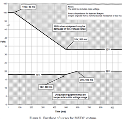
The voltage profile applied at Vin is given below . test start with 28V and switched to 100V(slew 100mS) and followed the below profile

  • Abilash,

    I'd be more than happy to help you troubleshoot this issue you're seeing with our design. As we didn't see anything like this in our own testing, we will have to do a little remote troubleshooting. I apologize if any of these questions seem low level, but I want to make sure that all the boxes are checked.

    You mentioned going up to 9A (with a 15A requirement) with the new FETs. Have you performed the SoA calculations to ensure that it will operate here correctly?

    By chance, do you happen to have waveform captures of the input, output, or any internal voltages during the testing?

    Are you able to share your layout so we can ensure there are minimal parasitics? 

    Regards,

    Bart Basile

  • Dear Bart Basile,

    We coudnt capture any wave form during the testing.

    SOA : The calculated Ids was around 12A for a 50mS pulse. We are planning to use MOSFET with better SOA also.

    We tested the similar test case in our lab with Load current of 2A , and captured some waveforms also.

    (Attached is the wave form at  first stage output (Yellow) and input volt at 88V)

    Best Regards,

    Abilash 

  • Abilash,

    By what metric are you qualifying the new FET as a "better SOA"? When comparing the SOA graphs of both devices, it does not seem to have better performance at long duration pulses. I do not expect it to perform in this application at 9A or 12A.