Other Parts Discussed in Thread: PSPICE-FOR-TI, , UCC27524
Tool/software:
Hello Everyone,
I was just looking into the TIDA-010216 reference design and trying to simulate the charging and discharging circuits using Pspice-for-Ti software. The gate driver IC's input pins are connected to a 50% duty cycle PWM signal, and I was expecting a boosted PWM signal with the same waveform (i.e., from 3.3V to 12V).
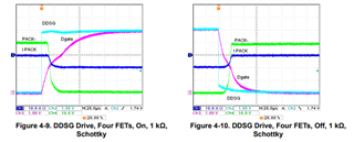
- However, as you seen in Figure 1) the output waveforms differ from the input PWM and there is a delay. So, I want to know the reason behind this, I mean why 1K ohm and 806-ohm resistors are chosen and why the waveform needed to behave this way?
- But as you can see from Figure 2) when I change the two resistors value to 75-ohm 75-ohm, the waveform becomes similar with the input PWM and there is no delay.
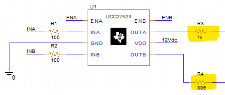
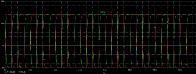
Figure 1) schematic and transient simulation result for 1K and 806 series resistors.
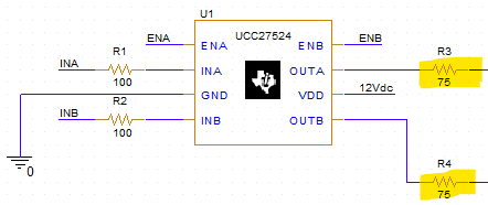
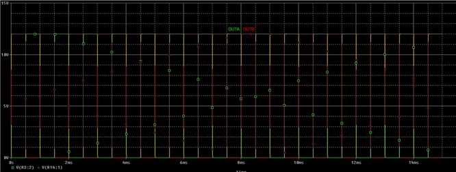
Figure 2) schematic and transient simulation result for 75 and 75 series resistors.