This thread has been locked.

If you have a related question, please click the "Ask a related question" button in the top right corner. The newly created question will be automatically linked to this question.

LM5122: Boost converter IC

Part Number: LM5122

Tool/software:

Currently for one of the Product we are using an Boost converter MPN: LM5122QMHX/NOPB,


Our requirement is as follows:

  • Input voltage: 12VDC
  • Output voltage: 80VDC
  • Output current: 0.6A


Attached is the circuit:

Problem that we are facing and want your feedback and corrective action:

  • With this configuration Mode connected to Ground, the device enters Pulse skip mode and during no load the output voltage is 80VDC,
  • When we start giving the load the output voltage gets reduced.
  • Also we changed the Mode by connecting the Mode pin to Vcc (connected a wire after left the mode pin and connect the other end to C202 Vcc pin side)
  • When the load current is less (0.15A), it enters in skip cycle the output voltage is not stable, we observed the following waveform at output and on the switch pin
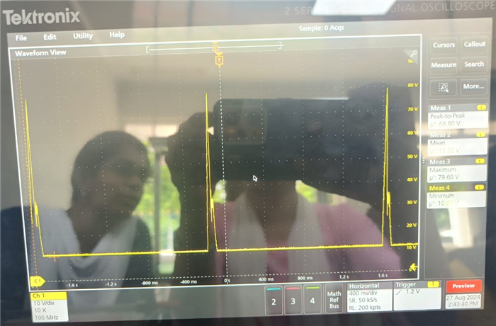
Output voltage at TP21.
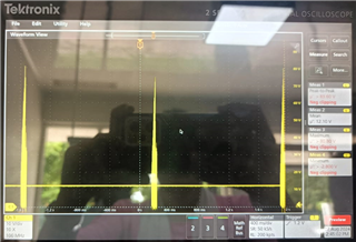
Voltage measured at SW pin.

  • When the load current is above 0.25A then the forced PWM is entered but the output voltage is not stable, please find the waveform:
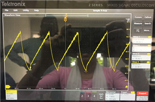
Output voltage at TP21 with Forced PWM.
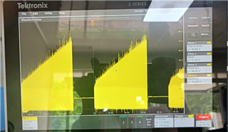
Voltage measured at SW Pin.

  • Since the switching cycle is not continuous and there is ramp the same time duration appear for the output voltage and when the switching cycle stops the output voltage starts to decrease we checked the duration it is OFF the ramp down time it meets.
  • Kindly let us know what component we have to change so that the switching cycle is continuous and there is no discontinuous.


Request you to kindly connect us to an application support team to help us in resolving this issue,


We need to deliver this an product for one of the Automotive application.

  • Hi Diana,

    Thanks for using the e2e forum and sending the waveform pictures.

    If the output voltage and switching signal is only stable in certain load conditions, it may be indicating that the compensation loop is not properly designed.
    The compensation is defined by R239, C204 & C207 at the COMP pin.
    C204 with 5.6nF might be too large and therefore leads to instability. You can double check the compensation with our Power Stage Designer tool, which comes with a compensation calculator. You can also calculate the compensation by hand using the formula from the datasheet.

    Please adjust the compensation and check if the behavior improves.

    Best regards,
    Niklas

  • Hi Niklas,

    Can you give us a correct capacitance value for compensation pin. We didn't get a stable output voltage . kindly, suggest some compensation values for resister & capacitor..

  • Hi Diana,

    Our engineer is currently out of office. Please expect an answer on Wednesday. Thank you.

    Best regards

    Yezi Yang

  • Hi Diana,

    Sorry for the delay.
    Here are some suggestions on optimization:

    - You can consider increasing the switching frequency to reduce inductor current peaks. Right now it should switch around 70kHz. I would recommend to go up to 300kHz or even 400kHz. (R242 from 133kOhm to 22.5kOhm)
    - For compensation network, I would suggest the following starting values:
    R239 5.23kOhm -> 47kOhm
    C207 100nF OK,
    C204 5.6nF --> 100pF

    Best regards,
    Niklas