This thread has been locked.

If you have a related question, please click the "Ask a related question" button in the top right corner. The newly created question will be automatically linked to this question.

TIDA-01187: Schematic Review

Part Number: TIDA-01187
Other Parts Discussed in Thread: THS4541, TLV3601, OPA857,

Tool/software:

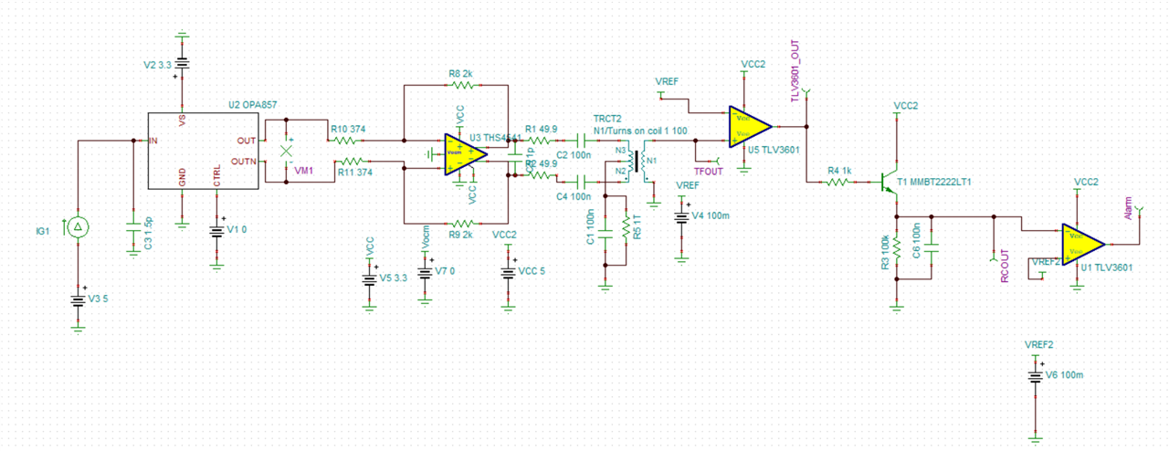
I Have taken TIDA-01187 as reference and built below schematic for optical to electrical conversion to a TTL output and also the same TTL output shall trigger a LOS signal

Requesting for your valuable suggestions

SIgnal Characters of mine are below

Min PW 50nS

Min PPR 1uS

Rise Time 1nS

Output Seen

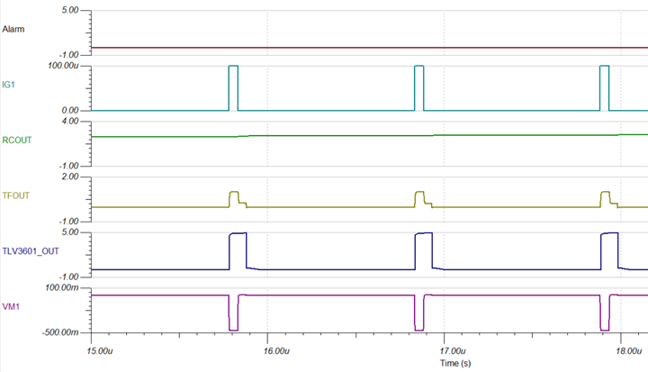
I deally the TF output should be clean to follow input and i am seeing pulse expansion on output side

Kindly let me know what changes need to be made to maintain the PW properly

  • Hi Shyam, 

    The issue is with the Vocm pin connection on the THS4541. Setting the Vocm to GND is driving the outputs of the THS4541 into saturation. Since you are AC coupled on the output I would just float the pin or set it to 1.65V. 

    Regards, 

    Jacob 

  • 3542.OPA857+THS4541+TLV3601_Anant.TSC

    I tried your suggestion, but it causes convergence error on TINA, Attached for your reference

  • Hi Shyam, 

    For now I removed the TLV3601 and that solved the convergence issue. I will work on trying to get the whole circuit to simulate. 

    The pulse expansion was being caused by the output of the THS4541 stage saturating. If you reduce the input amplitude you'll see that it no longer has an expansion. 

    I'll send you a different circuit shortly to try and allow for more input range. 

    Best, 

    Jacob 

  • Hi Shyam, 

    I made a few adjustments to the attached circuit to improve performance. 300uA into the OPA857 was causing the output to saturate so I reduced it to 240uA and also increased the rise and fall time as that was causing an overshoot on the pulse (I believe that is just a model issue). I also connected only the single ended input of the THS4541 and added a bias voltage to the other input. This doubles the total differential output swing on the THS4541 and I also adjusted the gain to achieve a 4.5V differential output signal. 

    To get the simulation to work I had to manually set the transient step time to a small value so the simulation time has increased. It seems that the TLV3601 model does not behave well with very fast pulses. 

    Best, 

    Jacob 

    3542.OPA857+THS4541+TLV3601_JF.TSC

  • I just wanted to check how circuit behaves with high current, but actually i am not working with such high current, i will work from 10u-100u Current band

    coming to TIDA-01187, the reference has differential output of opa857 going to input of ths4541 without this 1.25 v at input end, you have added for this high current cause?

    i dont think its required in my case, also i wish to work with TTL 5V so TLV shall have 5V as VCC, so i modified accordingly and i included an LOS signal output for my ease, hope this should work in real design also, let me know if you feel any additions are required before launching for design.

    OPA857+THS4541+TLV3601_WITH_LOS.TSC

  • Hi Shyam, 

    You don't have to make the modification between the OPA857 and the THS4541 that I shared. It is just optional if you wanted to get greater dynamic range out of the system. Here is an article that discusses the topic in depth. https://www.ti.com/lit/an/slyt773/slyt773.pdf

    I don't see any further issues with the amplifier. I will go ahead and reassign this to our comparator team to have them review your TLV3601 circuits. 

    Best, 

    Jacob 

  • Thanks Jacob!

    Hi Shayam,

    Your TFOUT on the first 3601 INP is about -100mV,

    our recommended & absolute input voltage range is -300mV from Vee (gnd in this case) so this does get a little close to that. 

    Besides that, the setup of our TLV3601's is fine.


    Please reply for any further assistance.

    Best,

    Michael

  • I simulated multiple limits of input current but could not create more than -100mV, let me in what case it may go up to -300mV

    do you have any alternative suggestions to TLV3601 in that case, or should i need to use any protection circuitry ?

  • Hi Shyam,

    Any of our comparators at this speed will have a max limit of -300mV. I also ran through some test cases and also didn't find any that is more than -100mV. You're also using an isolating transformer, so protection circuitry isn't necessary.

    Best, 
    Michael

  • i have one last doubt, not sure if can be resolved here or i need to open a new thread, below is query


    The Reference design doesnt use the inversion of signal as its anyways taken to tranformer for single ended conversion ? it doensnt matter ?

    What if my schematic is connected as below ?

    Also the Tranformer dots are connected to FDA differently in my simulation in comparision to reference does it make difference ?, i tried to connect the transformer as shown in reference design it has failed

    My deisign which worked in simulator

    In my case as the OPA is giving out inverted signal, it is given to THS4541 for singal inversion and to T/F for single ended conversion, i have done scheme exactly same as simulation, even while connection the transformer(dots go to inverting output), reversing this failed the simulation.

  • Shyam,

    Because of the holidays, TI E2ETm design support forum responses will be delayed from Dec. 25 through Jan. 2. Thank you for your patience.

  • Shyam,

    Tranformer dots are connected to FDA differently in my simulation in comparision to reference does it make difference ?,

    Yes, the dots matter. otherwise the signal may be inverted. 

    Do you want an inverted output?

  • I tried to follow what is there in reference, From datasheet of OPA857 the ouput is inverted as understand.

    In Reference design the inverted output is directly given to THS and then to transformer, i feel the T/F is doing the inversion here please confirm

    I rebuilt same in simulation as in reference design , i did not see it working, there was a convergence error

    Now my design scheme is attached in above screenshots and also below, where inverted output of OPA857 is given to THS4541 for inversion, the output from THS4541 is non inverted signal, now the transformer dot is connected to -ve so that the output is non -inverted, please confirm this scheme, i feel it should be working as it worked in simulation,

    but i am not able to get exact equivalent symbol of transformer in simulation, hence confusion

  • Shyam,

    The diode polarity sets the input photo leakage current polarity. OPA857 input is inverted such that 'current in' becomes OUT voltage going lower and OUTN stays still. So related to photo current flow, OPA857 OUT is inverted.

    In figure 18 of design guide. The un-inversion happens at THS4541 outputs, see the dot on the top side. Top, bottom swap.

    The above is fine. The below is not fine. Pins 10 and 11 are swapped.