This thread has been locked.

If you have a related question, please click the "Ask a related question" button in the top right corner. The newly created question will be automatically linked to this question.

TIDA-01606: Ask for advice on parts changes

Part Number: TIDA-01606
Other Parts Discussed in Thread: SFRA, UCC21710-Q1, UCC21710

Tool/software:

Hello,

Please tell me, because we want to provide greater power, we changed the CASR 15-NP to CASR 50-NP of U3/U4/U5

Is there anything that needs to be adjusted in the software?

Because the values now read from TINV_iGrid_A_sensed_Amps / TINV_iGrid_B_sensed_Amps / TINV_iGrid_C_sensed_Amps are only about half of the values asured by the instrument?

Sorry to trouble you, thank you

  • Gavin,

    You will have to update the max parameters (i.e. for scaling) in main.syscfg.  This will automatically update the tinv_settings.h


    #define TINV_IINV_MAX_SENSE_AMPS 
    #define TINV_IGRID_MAX_SENSE_AMPS 

    The ADC readings are normalized to the full scale accordingly to the ADC VREF.  For example, if the VREF = 3.3V you have to calculate what is the current at the input required to reach 3.3V at the ADC input.   This is defined in the TINV_IINV_MAX_SENSE_AMPS in main.sycfg.  For AC reading, the SW normalize the ADC reading from -1 to 1 and then convert to AMPS with the TINV_IINV_MAX_SENSE_AMPS. From tinv.h:

    //
    //

    #if TINV_CURRENT_LOOP_SENSE_OPTION == TINV_ADC
    TINV_iInv_A_sensed_pu = ((float32_t)TINV_IINV_A_READ * TINV_ADC_PU_SCALE_FACTOR - TINV_iInv_A_sensedOffset_pu) * 2.0f;

    //
    // convert the pu values to volts and amps
    //
    TINV_iGrid_A_sensed_Amps = TINV_iGrid_A_sensed_pu
    * TINV_IGRID_MAX_SENSE_AMPS;
    TINV_iGrid_B_sensed_Amps = TINV_iGrid_B_sensed_pu
    * TINV_IGRID_MAX_SENSE_AMPS;
    TINV_iGrid_C_sensed_Amps = TINV_iGrid_C_sensed_pu
    * TINV_IGRID_MAX_SENSE_AMPS;


    Is CASR 50-NP the only current sensor you're using? Do you have the shunt current sensor (AMC13x) on the GRID side like the reference design?

    Increasing the power for the design will require you to update many things including the inductors and capacitors, thermal management, and layout etc.  I assume you already did this analysis?

    -kelvin

  • thanks for your reply
    We hope this kit can provide an output of 15KW (maximum possible 18KW)
    Yes, completely use the circuit of the reference design and modify the following parts to comply with the output can reach 440V (L-L)
    1. CASR 15-NP -> CASR 50-NP (u3/u4/u6) (CASR 50-NP is required?)
    2. 2m -> 1m (R5/R41/R47)
    3. L1/L3/L5 increase current
    4. L2/L4/L6 increase current
    5. C8/C9/C10 improve withstand voltage
    
    What I want to ask is "VREF = 3.3V, you must calculate the input current required for the ADC input to reach 3.3V" How to calculate?
    Or maybe what we should adjust is the multiple of OPA?
    
    
  • Gavin,

    If you look at the datasheet, the gain for the CASR 50-NP sensor is 625 mV / Ipn, where Ipn is the primary nominal RMS current (50A in your case).  That is the gain is 12.5mV/Arms.  I assume you have a difference amplifier similar to the reference design (which has a gain of 1).  This means that the signal chain gain is just 12.5mV/Arms.  The difference amplifier midpoint is 1.65V (0A input).  So to get to the theoretical FS ADC input of 3.3V you need 1.65V/12.5mV/Arms = 132Arms or 186A peak.  In the syscfg file, you would put 186A as the maximum current, this will calibrate your SW gain.  

    But keep in mind that the CASR 50-NP is limited to +/150 A peak operation i.e. 106 Arms (i believe it's to operate in the linear region) as stated in the pg.8 of datasheet.  The abs max output of this is +/-170 A i.e. 120.2 Arms  peak (including nonlinear operation).

    So that means that the ADC would only see a maximum voltage of 1.65V + 106Arms*12.5mV/Arms = 2.98V (linear operation of sensor) 

    -Kelvin

  • Hi Kelvin,

    First of all, thank you for your help. I have some other questions to ask.
    1. When the three-phase voltage in lab2 is under light load, the voltage will increase outward. )
    2.In tinv_37x.h
    TINV_vGrid_A_sensed_pu = ((float32_t)TINV_VGRID_A_READ *
    TINV_ADC_PU_SCALE_FACTOR -
    TINV_vGrid_A_sensedOffset_pu ) * -2.0f
    In tinv_37x.c, you can find
    TINV_vInv_A_sensedOffset_pu = TINV_VOLTAGE_OFFSET_PU;
    TINV_vInv_B_sensedOffset_pu = TINV_VOLTAGE_OFFSET_PU;
    TINV_vInv_C_sensedOffset_pu = TINV_VOLTAGE_OFFSET_PU;

    TINV_vGrid_A_sensedOffset_pu = TINV_VOLTAGE_OFFSET_PU;
    TINV_vGrid_B_sensedOffset_pu = TINV_VOLTAGE_OFFSET_PU;
    TINV_vGrid_C_sensedOffset_pu = TINV_VOLTAGE_OFFSET_PU;

    Can I give different values the offsets of these six values?
    We hope that the value of sw does not differ too much from what is measured by the instrument?

    3. You will hope to minimize this error in lab2
    The main reason is that when we use lab4 to connect to the grid, the grid connection at 110v seems to be successful.
    However, when connecting to the grid at higher voltages (such as 150V/180V/220V), the entire waveform will be completely distorted.
    We wonder if the grid connection fails because the error value is too large?

    4. When using lab4 to connect to the grid, is the correct shutdown procedure to turn off the AC source first and then the DC source?
    Because when we turn off the AC source, the entire waveform will be completely distorted (looks like out of control?)
    Or do we need to turn off the relay first and then turn off the AC and DC sources?

    5. I would also like to ask, how to confirm the current status of the power grid when connecting to the grid? In our understanding, after relay is turned on
    Aren’t the three-phase voltages output by the inverter and those from the grid mixed together?

  • Hello happy new year:D
    Ask for advice
    1. In Lab4, when we connect to the grid, according to the file instructions,
    When the grid voltage does not reach 230Vrms (currently we use 110Vrms), TINV_startStage = 1 must be turned on
    When Vrms=230, turn on TINV_allRelaySet=1, but during this process we keep encountering the situation where the resistor is burned.
    2. We adjusted the program so that when Vrms=230, first turn on TINV_startStage=1, wait 500ms and then turn on relay.
    However, it is observed that TINV_powerRms_A_Watts is a negative value in CCS expressions? Can't it be used like this?

  • Gavin,

    Lab 4 uses TINV_idRef_pu to control the output of the inverter similar to Lab 3.

    The higher the TINV_idRef_pu value, the higher the output voltage of the inverter.  The resistors will burn out if you turn on the GRID and if you wait too long for the relay to turn on (try to turn on within 2 sec).  If you examine the circuit, you will see that the EMI filter stage is basically a reactive load if your GRID is on.  Hence, the resistors will heat up, especially at 230Vrms.  You can fix this by using larger inrush resistors.  Please calculate the power loss of the reactive load at 230Vrms & 60/50 Hz.  Please take care of the resistor power rating issue first.  

    In lab 3, when you test the inverter with resistors what was the sign of the TINV_powerRms_A_Watts reading? I believe if the inverter is pushing power to a load, the TINV_powerRms_A_Watts should be positive.  If it's negative, I think you need to increase the TINV_idRef_pu.  Negative power means power flowing into the DC Link as in the PFC mode.

    Are you using a Chroma to emulate the GRID?  

    From lab 3, you see that for a given TINV_idRef_pu, different resistive loads will give you different inverter output voltages.  You're basically controlling a current source.  So if the "GRID" impedance is lower than lab 3 resitors, you might not be able to use the same TINV_idRef_pu value.  Do you have an idea of the GRID impedance?

    What is the proper shutdown sequence:

    1. If you turn off the inverter PWM or TINV_idRef_pu = 0  with the GRID still connected AND keeping the relays ON your inrush resistors will be safe.  Next, you can turn off your GRID AC source.  If your AC source is a Chroma, it will probably have its own relays as well when turned off.  Next, turn off the DC source.  Finally, you can turn stop the debugger in CCS and power down the aux 24V supply.

    btw, i would recommend you either increase the power rating of your inrush resistors or use a PTC thermistor for inrush protection PTCEL13R600LBE.

    note: In lab 4, when you turn on the power stage, the inverter is supposed to lock to the GRID frequency (PLL).

  • BTW, what end equipment / application are you designing for?

    Happy new year to you as well!

  • Hello,
    Our current main application is similar to diesel generators.
    The 330Hz~380Hz AC power generated by the generator is converted by the generator chip tida-01606 into AC->DC (>=800V DC), and then DC->AC (220V 60Hz)
    In fact, time is very urgent. It is expected that we will have 24 films (12 episodes) back to the company in the next two weeks.
    Next month it will be 1,000 pieces (500 sets).
    So any changes to the hardware we hope to have completed by the end of the month.
    
    
  • Hello,
    Thanks for your suggestion to turn off Lab4, the burnout of the resistors has improved significantly now!
    Also, I would like to ask some questions. We encountered some problems in the laboratory.
    When the value of TINV_idRef_pu is preset to 0.005, the grid connection will successfully load the current to the grid,no matter it is between DC400V ~ DC800V (AC110 ~ 220V).
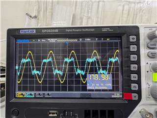
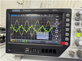
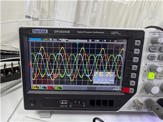
    When the value of TINV_idRef_pu is increased to above 0.2pu, abnormal noise (similar to current) will be heard on the power baseboard, and then the AC output will appear as follows?
    Equipment currently used:
    DC: Chromium 62180D-1200
    AC: Chrome 61815
    Vbus Max sense  1144
    Vgrid Max sense 450
    INV Max sense   132
    INV trip limit  106
    Igrd max sense  64
    Igrd trip liumit 35
    I would like to ask, do you have any other suggestions that can help us? thank you
  • Hello 

    I went to test the harmonics today and found that the limits were exceeded at high frequencies.
    I don’t know what suggestions you can give in this regard? (hardware or software)
  • Hello 

    When testing harmonics today, we used the above settings to adjust the maximum power to 14KW (850V DC/ 254V AC out)
    But when TINV_idRef_pu >0.34 (14KW), the power baseboard will stop output. So are there any suggestions for modifying the above setting values?
    In addition, the following two values ​​were modified:
    Power
    Rated:17000
    Operating:15000
    Thanks:D
  • Just to confirm, are you using the same electrical design for voltage sensing and current sensing as the 1606 reference design?  The  polarity of the sensing matters.  In the SW (tinv.h, starting at line 405), we have the code inverting the voltage sign because the reference HW uses inverting voltage sensing.

    Have you tested your HW in lab 3 at various operating conditions like voltages (output 230Vrms) and power (14kW)?  Lab 3 uses resistor load so you will have to have a load that can handle that kind of power. Please use lab 3 to get comfortable with the HW and SW and only then move to lab 4.

  • Gavin,

    Please note that F28379D example SW uses sinusoidal pwm control and the F280039C example uses SVPWM.  

    F280039C example code has voltage regulation for the middle point of the DClink, which is good for unbalanced AC grid cases.

    Are you referring to the line current THD?

    -Kelvin

  • According to the information given by our hardware engineer, except for the following component changes, the circuit design and components of the hardware are all the same as those of tida-01606 (including layout)
    1. CASR 15-NP -> CASR 50-NP (u3/u4/u6) (CASR 50-NP needs to be enabled?)
    2. 2m→1m (R5/R41/R47)
    3. L1/L3/L5 maximum power
    4. L2/L4/L6 maximum power
    5. C8/C9/C10 improve withstand voltage

    The control card used is F28379D
    DC voltage provided by Chromium 62180D-1200
    The current loads used are Chrome 61815
    Yes, I mean the current THD will exceed the limit value at the 35th to 36th time.

    When we are in Lab3, due to time constraints (I have been working on this job for about 3 months now, there are actually many things I don’t understand) the voltage difference of each phase will be relatively large during the test.
    So we have been testing at low voltage (380VDC~600V DC)
    Mainly because of the instability of the three-phase waveforms, and the difference between the Vrms/Irms values ​​seen from debugging and the values ​​obtained from the instrument at high pressure, we paused the Lab3 test first.
    Due to time pressure, we urgently need to do harmonic testing, so we went directly to Lab4 (we successfully tested DC850V AC254V for the first time today, running between 12KW~13KW for more than half an hour to test harmonics)
    We changed a few things during testing today.
    1. Input DC 800V, confirm power on and then increase to DC 850V
    2. First input 110V to the AC terminal and make sure the relay is open.
    3. Increase the value of idref_pu from 0.005 -> 0.1
    4. Increase AC to 220V to confirm that the power output is normal and then increase to AC 254V.
    5. Slowly increase the value of idref_pu to 0.33 (about 13.7KW)
    6. When idref_pu reaches 0.34 (power exceeds 14KW), there is no output immediately.
    7. Directly set idref_pu=0, turn off AC->turn off DC
    My question is, if the starting idref_pu is set higher from the beginning, can the AC end give AC 254V from the beginning?
    Because when idref_pu=0.005 was used in the initial test, AC254V had no power output.
    Thank you very much for your help

  • A few comments:

    1. The 1606 reference design layout was design to support 16Arms of current.  If you want to support higher current, the trace width and thickness must be accounted for and derated for temperature.  There are many online calc tool to help you with this trace width estimation given a current and temperature delta target.  Is this accounted for in your new design?

    2.  I'm concern about the instability of the waveform you saw in lab 3.  This tells me that you haven't got the right compensation values setup.  When i was testing my new design, i had to tune the compensation parameters using COMPENSATION DESIGNER in the main.syscfg.  It's going to be a trade off between the control loop bandwidth and phase margin / stability.    Play around with the Kdc and fz0 values until you get a stable response.  It should be apparent when you get a stable response.  Do not proceed until to high power you stabilize the control loop.

    3. Throughout these tests, make sure to keep an eye on the watch window TINV_boardFaultFlags.  If there is a fault, the PWM will stop and you may have to reset.

    4.  I assume you have updated these parameters in tinv_user_settings.h according to your requirements:

    #define TINV_VBUS_OVERVOLT_LIMIT 900
    #define TINV_GRID_OVER_UNDER_FREQ_LIMIT 3
    #define TINV_GRID_OVER_UNDER_VRMS_LIMIT 35
    #define TINV_UNIVERSAL_GRID_MAX_VRMS 240
    #define TINV_UNIVERSAL_GRID_MIN_VRMS 20
    #define TINV_UNIVERSAL_GRID_MAX_FREQ 65
    #define TINV_UNIVERSAL_GRID_MIN_FREQ 45

    If you don't update these, you might get a fault trip.

    5. I'm not sure why you can't go directly to 254Vac.

    -Kelvin

  • TIDA-01606E7(001)_Sch.PDF

    Gavin, 

    I'm attaching an updated reference design schematic for 1606 (E7) .  The E7 EMI stage example on pg 4 is improved compared to E6. You can ignore the TPSF12C3DYYR (active EMI filter device) as it's a placeholder.  The important difference i would like to highlight here is the AC coupling from V_SN_N to VDC_MID via C67, C71, C72, C73, C75, C76.  In the E7 design we have GRID_GND or EARTH connection for common mode filtering.  This was missing in E6.

    I just thought that this might be a factor in the THD result.

    btw, the pdf is clickable.  you can find the P/N for the parts by clicking on them.

    -Kelvin

  • another hint: when combing through the code, i like to use CTRL H on the keyboard to search for variables in the project. For example, I can search for TINV_VBUS_OVERVOLT_LIMIT and see which file has it used. This helps me navigate around the large project and understand it better.  It's a big design, and it does take a bit of time to understand the HW and SW.

    In fact, i came across a couple of issues when bringing up my E7 board, one of them was getting the voltage sensing polarity wrong in HW. Another one is mitigating EMI.  Using ferrites at the inputs of the isolated DCDC bias supplies help a lot with EMI.  Lastly, in the E7, I ended up connecting the MCU ground to the EARTH GND via a ferrite instead of a 0R resistor to help with mitigating noise.

    Also, make sure you have enough airflow to cool your power stage heatsinks.  at 10kW, you can expect to get around 200W of losses from the SiC Fets. 

    -Kelvin

  • Gavin,

    Another place you need to consider is the ripple current rating of your film caps.  In the E7 design, we used 4x 3.9uF film caps (2x from DC+ to VMID and 2x from VMID to DC-) to support 10Arms of HF ripple current.  This HF ripple current is based on our PLECS simulation.

      If you don't have the right film caps for the given current rating, your THD might be distorted.

  • Hello
    Yes, we have updated the value of user_setting.h

  • Hello,
    1. Yes, after asking our hardware engineer, the answer is that we have thickened the layout circuit to support greater current.
    2. Regarding the compensation parameter adjustment part of the compensation designer, in fact, we have been unable to determine what kind of situation is good? What kind of situation is relatively bad? So we can only adjust a relatively similar one based on the graphics in the user manual. Replace it with the value of the graphic. Do you have any good suggestions for this part?
    3. The reason why we don’t use AC 254V directly is that we bring two boards
    The first one was directly connected to 850V DC. When connected to 254V AC, the B-phase resistor overheated and burned. After the resistor was repaired, the B-phase output did not work (later it was confirmed that the mosfet was also burned. I saw a beam of fire flying in front of my eyes at that time)
    Therefore, in order to ensure that the experiment can be carried out, we will increase the voltage from low to 110VAC -> 220VAC -> 254VAC, 600VDC -> 800VDC -> 850V DC on the second piece (only two power baseboards were brought that day)
    If the resistor is burned out, we will consider replacing it with a thermistor. Test again to see if the situation improves.
    The first problem with the power backplane was that the specifications of the MOSFETs were modified according to the hardware engineer’s reply.
    C3M0060065D modified to C3M0045065D
    C3M0075120D modified to C3M0032120D
    But in the current test in Lab2, as soon as this base plate exceeds 10KW (the same image can reach 14KW on another unmodified mosfet), the output will drop.
    However, using simulation software to see the effect, the heat dissipation and efficiency after replacement will be better. I don’t know what suggestions you have in this regard?
    4. We are currently using the E6 version of the design. Since 1,000 pieces have been shipped (it seems that the circuit boards have not been washed yet), we are not sure if it will be time to modify it. However, this design drawing is still of great help to us. If possible, we I will discuss with the manufacturer to see if it can be made later.
    The first 24 tablets can only be used with tears in eyes (scheduled to arrive around January 15th)
    5. Another question I would like to ask is, can the timer #define TINV_ISR2_TRIG_BASE CPUTIMER2_BASE in tinv_user_setting.h be changed? (Currently using F28379D)
    I found a modbus reference example from Ti's forum, which uses timer, so I set it to timer2. As a result, Vrms/Irms are not displayed XD
    6. We hope that the speed of this Fan can be controlled periodically, so we set the original Fan switch GPIO9 to GPIO_9_EPWM5B. Will this have any impact on the system?

    There are a lot of questions, I hope they won’t cause you any trouble
    Thank you very much for your help.

  • for the compensation, you will have to play around with the values.  Starting with the values shown in the user's guide is a good start.  you will see the current waveform changes with each new compensation values.  A stable system will have minimal spikes in the waveform.

  • you mentioned the output dropped...were there any faults reported on the ccs watch window?

    you can try to pwm the fan. emi from the power stage could affect your fan from working properly. you might have to use snap ferrites 

  • Hello,
    There was a problem that the power could not reach 15KW. Later, after the hardware engineer made reinforcement welding on the PCB pins, Lab2 can now run stably at 15KW.
    But for Lab3, as long as the voltage is above DC 600V, there will be a high chance of fault_iInv (A/B/C)_overCurrent=1? why ?
    In addition, we are reading the value of TINV_iGridRms_(A/B/C)_sensed_Amps.
    The value of TINV_iGridRms_A_sensed_Amps is much smaller than the actual value.
    The deviation of TINV_iGridRms_B_sensed_Amps will be between A/C.
    The value read by TINV_iGridRms_C_sensed_Amps will be closer to the actual value.
    Does this have something to do with the distance between the sensor and the control card?

    thanks for your help

  • Hi,
    Have a question?
    Why does F28379D not use SVPWM? What are the factors to consider?
  • Gavin,

    sorry i was OOO for a few weeks.  now im back.  

    When the 1606 was first released with the 79D controller, the previous engineer decided to use sinusoidal pwm control (perhaps due to simplicity).  

    the latest release with 39C support, we decided to use SVPWM due to a number of benefits.  The key trade offs between SPWM vs SVPWM can be found online:

    Sinusoidal Pulse Width Modulation (SPWM) and Space Vector Pulse Width Modulation (SVPWM) are both techniques used to control the output voltage of a three-phase inverter, but the key difference is that SVPWM generally provides better utilization of the DC bus voltage, leading to lower harmonic distortion and higher efficiency compared to SPWM, which generates a more sinusoidal waveform by comparing a sinusoidal signal with a triangular carrier wave; making SVPWM a more advanced control method, although it is also more complex to implement.

    -Kelvin

  • Hi nice to meet you again!

    So if we have new projects to work on in the future, we should consider using 39C instead of SVPWM.

    In addition, I would like to report to you that we still have some problems.

    In Lab2 we have tested that it can run on 15KW for a long time. (Although its ADC has always been inaccurate)

    Lab3, currently we want to understand how to adjust SFRA first, so we pause first. What we have seen before is for example: A-phase voltage 100V, B-phase 60~70V, C-phase 110 (close to the actual value)

    Lab4 can be connected to the grid, but the maximum power is only 14KW, and there are still problems with harmonics and AC and DC. I will wait for Lab3 to be adjusted before testing again.

    Lab5 can start PFC at 30Vrms. The userguide found that it can only be tested at 30Vrms. Can it be tested at 230Vrms? (We currently encounter overcurrent problems at 100Vrms)

    Lab6, by adjusting the load and test method, you can execute SFRA at 230Vrms and get a normal-looking pattern:D

    Lab7, use the TINV_GI_PI_KP TINV_GI_PI_KI adjusted by Lab6 to continue to do SFRA. It can currently reach 12KW (overcurrent errors will occur later)

    Regarding the adjustment of SFRA, I have some questions to ask you.

    1. Some documents suggest PM>45 deg, GM =6 dB. Is this really the case?

    But the pattern of lab3 sfra in UG, PM: 44.69deg, GM: 18.23 dB? (3-13)

    Lab4 PM:37.33 deg GM:5.02dB ?(3-15)

    Lab6 PM:64.73 deg GM:16.56 dB(3-28)

    Lab7 PM:41.81 deg GM:52.27dB(3-32) why??

    2. The frequency values ​​look different. How many are correct?

    3. Figure 3-22 When we design compensation, should the red point be to the right of the 0dB intersection? Or to the left? Will this have any impact?

    It's still nice to see you again to answer questions, thank you :D

  • Yes, we recommend 39C for new projects.

    For the ADC measurement accuracy, what is your ADC voltage reference? If you're using a 3.3V power rail for your adc reference, this can have significant impact on the accuracy 

    I actually haven't gone through the SFRA function myself so i can't give you insight on this yet.  I was able to tune the loop with just the compensation tool.

    With that in mind, i believe the 39C example code doesn't have the SFRA included...

    Lab 5 was meant to be a quick test before going to higher voltage and power as in lab 6.  Lab 5 doesn't require loop tuning to be done since it's just for verifying basic boost functionality.  If you have the current loop tuned i don't see a problem with running lab 5 at higher voltages.  Now if your current loop isn't tuned properly, the high gain can cause OC issues as you can imagine.

    for phase and gain margins, the recommended margin are between 45-60 degrees and 6-12 db for gain.

    i agree that some of these SFRA results are not ideal.  I'm not sure why they had these results shown here as the phase margins are not at least 45deg.

  • Hi,
    I'm bothering you again!
    Yesterday I asked a question about frequency.
    Because when referring to some documents, it is stated above that Fc = 1/5~1/10 of the off frequency? (about 5K~10KHz)
    However, another document mentioned that when PFC is used, Fc = 10~20 times of 60Hz (600~1200Hz)
    The reference Ti file shows about 600Hz, but after running SFRA, the frequency shown above is about 1300Hz (it seems to be 10~20 times of 60Hz)
    However, here comes the problem.
    When I start the PFC, set the negative voltage to 3.18K, AC=220V
    1. open relay
    2. tinv_idref_pu = -0.013 (later revised to -0.009, because -0.013 vbus will exceed 900V DC)
    3. startpowerStage, vBus will change drastically at this time. From nearly 900VDC->850VDC (stable)
    So in Lab6, I started with AC 180V and then boosted it to 220VAC, but I think this is wrong.
    So does this have anything to do with frequency?

  • gavin,

    As a rule of thumb, you would want to set your AC current & voltage sensor HW filter cut off frequency to be a couple of decades away from the grid frequency.  I would be okay with anywhere from 20x to 100x for Fc.  This is to minimize phase error from the filter stage over operating conditions for power factor correction reasons.  For the grid Point of Common Coupling PCC measurements, 5kHz should be fine.  You can add SW filter later if you want to further reduce noise (e.g. averaging).  But keep in mind HW filter is the only stage to target large noise spikes (if you expect them to be there) before it can alias into your sampling.  Once aliased in baseband, SW filtering can't really do much.  there are a lot of material online that talks about aliasing.  Just to give you a heads up on HW vs SW filtering.  There are things you can't do in SW.  For anti-aliasing, you can use LP HW filtering and increase the sampling freq.

    For the switching node current sensing, from a control perspective, you might want to have a bit more BW so 20kHz would be fine.  you could easily change the cutoff later on so it's not a big deal.

    Note, don't get confuse about the filter cut off versus an RC charge bucket at the output.  the charge bucket has much smaller RC values to help drive the ADC to LSB/2.  it basically reduces your op amp BW requirement for a given N-bit ADC and VREF.  TI has an analog designer tool that helps you with the charge bucket design to interface with SAR ADCs.

    -Kelvin

  • Hi
    I’m here to ask some questions again,
    1. In the user guide of tida-01606, Page 70. How to set the FED_SOFT_START shown in Figure 3-26?

    2. When using a current probe to observe the current waveform, when setting TINV_startPowerStage, the current waveform will be seriously distorted. Is this normal?

    3. When testing in Lab7, when the output reaches 8KW, the current waveform will change from the positive and upper waveform? What do you think is the possible reason for this?

    Thank you for your help and I hope you can give me some suggestions.

  • Hi

    Please advise,

    We recently manufactured a batch of tida-01606 and found a problem, that is, the output power is less than the expected 15KW !

    Later, we increased the Deadband (in uS) to 0.2 to reach 15KW, but according to the datasheet, the MOSFET used only needs to be set to 0.1us, which should be enough.

    Do you want to know what effect increasing the Deadband will have on the system?

    BR,

    Gavin

  • i will get back to you soon

  • 1. I'm waiting for my colleague to see if he knows about the softstart feature in the code.  I couldn't find it myself on first look.

    2. that current waveform is not normal.  that looks like an unstable system.  you need to tune your compensation until you get a nice sinusoidal current profile.

    please adjust the gain and bandwidth.  the system tends to be more stable when you decrease the bandwidth but this may affect your transient performance.

    3. can you confirm that you have correctly calibrated your current sensors with the right ABS max settings?  also, your controller ADC references are configured to 3.3V?

    In general, increasing deadband will increase distortion (THD).  For my E7 board, we got the board to work at 150ns.

    -Kelvin

  • Gavin,

    about the softstart feature, you might want to check out the TINV_HAL_updatePWMDeadBand function usage in tinv.h

    -kelvin

  • HI,

    May I ask, what does ABS in right ABS max settings mean?
    Speaking of the E7 board, can this board support up to 30KW? Or does TI have other solutions that can support up to 30KW? We are currently evaluating the next version (to complete the development and verification of 30KW before the end of this year). If there are no surprises and no choice, then we will continue to use the E7 version of TIDA-01606. Then strengthen the voltage and current resistance...

    In addition, I will find time to check TINV_HAL_updatePWMDeadBand again. Thank you for your help.

    Finally, I would like to ask your opinion. In Lab3/4/67/7, we all encountered the same problem, that is, the maximum power can only be below 14KW? The same problem is that we encounter overcurrent. Is the possible reason still the adjustment of SFRA? Or is there anything we need to pay attention to in the hardware?

    BR,
    Gavin

  • Hi

    We are now encountering a strange phenomenon. When the output is 14KW, the hardware protection will jump regardless of the PFC or inverter mode!
    Are there any places that we haven't noticed?

    BR,
    Gavin

  • Gavin,

    In general, this 3L T type topology can support 30 kW.  An example would be this 25 kW t-type design from wolfspeed

    If you want to support 30 kW using E7 1606, you will need to consider new current sensors, magnetics, capacitor, and pcb layout.

    In our tests, we only tested our design up to 11kW due to the limitation of our test equipment and also our design requirements from the start.

    Were you able to capture the overcurrent event with the scope?

    are you using both the hall current sensor and shunt based AMC sensor?

  • sorry ABS max means absolute maximum.  I'm referring to the setting in the syscfg file.  these values like the VBUS MAX SENSE sets the max measurement range.  in the code, everything is done is relative terms (-1 to 1 for AC and 0 to 1 for DC).  the code then use the VBUS MAX SENSE with the relative term to convert to actual voltage.

  • Hi,
    yes, we use hall current sensor and shunt based AMC sensor at the same time. It may be a bit difficult to capture overcurrent events with an oscilloscope. We use current probes to monitor, but we never see overcurrent?
    Is this related to the unevenness of the three phases? Our actual measurement found that each phase has a difference of nearly 1Amp, such as A phase 10A, B phase 11A, and C phase 12A.
    Especially when we use chroma instruments, it can reach 14KW, but when connected to the grid for grid-connected testing Only available to 8KW..
    BR,
    Gavin

  • Hi,
    would you like to ask, does the FLT signal from the gate driver have anything to do with UCC21710-Q1? (Our rating is 15KW)?
    BR,
    Gavin

  • possibly...there's a DESAT OCP feature with UCC21710.  If you're increasing the drain current, you will have to determine the appropriate DESAT threshold for your new design.

    check out this gate driver calc tool to help you with the DESAT design:

    https://www.ti.com/tool/download/SLUC695

    you would want to align your VOCDET (from the spreadsheet tool) to the IV curve of your SiC FET.

    If you set the voltage too low you may trip more often due to current spikes.  There is a blanking time in the circuit as well.

    -Kelvin

  • Hi,

    We use the gate driver calc tool to adjust the voltage of the VOCDET to the same as the E7 version (about 4V), and also adjust it to a larger voltage (about 7V). The result is the same. The power can only reach 13~14KW. If it exceeds 14KW, the red light of the hardware FLT will jump.
    So should the voltage value of R2 be increased or decreased? According to your previous reply, it should be increased, right?
    In addition, the hardware flashes the red light of FLT, but the software does not give any warning? Is there something wrong with my settings?
    BR,
    Gavin