Because of the holidays, TI E2E™ design support forum responses will be delayed from Dec. 25 through Jan. 2. Thank you for your patience.

LMG3422R030: LMG3422R030RQZT

Part Number: LMG3422R030
Other Parts Discussed in Thread: LMG34XX-BB-EVM, LMG342X-BB-EVM

Tool/software:

Dear Team,

I hope this email finds you well.

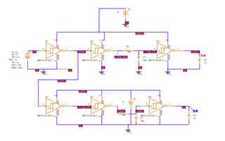
We recently purchased the LMG342XEVM-04X evaluation board, and I am currently verifying the schematic by simulating the circuit used for generating complementary signals with a dead band. However, I have encountered an issue during the simulation.

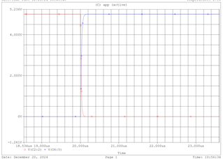
Specifically, I noticed that the rising and falling edges of the complementary signals are occurring simultaneously. As a result, there are instances where both signals are momentarily ON at the same time. From my understanding, this behavior is not expected. At any instant, the two complementary signals should not turn ON simultaneously. Instead, the signal that is about to turn OFF should turn OFF first, ensuring a safe dead time before the other signal turns ON.

Could you please clarify how the dead-band circuit in the schematic ensures proper operation? If there are specific configurations or settings that I need to consider during the simulation, I would greatly appreciate your guidance.

 Hera i am attaching simulation results for your reference

Thanks and Best Regards

Hareesh

  • Hello Hareesh,

    I can definitely help here, I have a few questions:
    1. We have two buck/boost motherboards (LMG342X-BB-EVM and LMG34XX-BB-EVM), however LMG3422 EVM is compatible with LMG342X-BB-EVM, are you using this motherboard and basing your simulation with it?
    2. The LMG342X-BB-EVM motherboard can be configured to use either single input from low side or dual input with both high and low side. I assume since you are simulating a signal splitter with deadtime that you are using single input. But can you confirm?

    Two actions for you:
    1. Add a diode across R1 and R3, this will allow rise voltage 5V to pass directly without delay. We add delay to the fall time on both the high and low side. Since the signals are inverted the fall time of the high side will account for the deadtime on the rise of low side and vice versa.
    2. Please send a more clear image of the schematic after adding diode, it will help me review easier

    Thanks,
    Zach Soviero

  • Dear Zach Soviero,

    I am currently working with the LMG342X-BB-EVM motherboard and simulating the schematic provided in its reference manual. As part of my setup, I am using a single input and deriving a complementary signal with dead time from it.

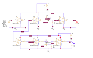
    Based on your guidance from the previous email, I have incorporated the suggested changes by placing diodes across R1 and R3 in my schematic. However, despite implementing these modifications, I am still unable to achieve the proper dead time in the circuit.

    Could you kindly assist me in resolving this issue? Any further insights or recommendations would be greatly appreciated.

    Thank you for your continued support, and I look forward to your valuable guidance.

    Here i am attaching schematic and results

    Thanks and Best Regards

    Hareesh

  • Hello,

    I am happy to further assist you with this, I can even run a simulation myself to see what differences there may be; however it will need to wait until week of Jan 1st after US holidays. I hope this is acceptable for you.

    In the meantime, please continue to debug and share any additional information you uncover.

    Thanks,
    Zach Soviero