LMG3422R030: LMG3422R030RQZT

Part Number: LMG3422R030

Tool/software:

Dear Team,

I am currently working with the LMG3422R030 GaN FET using the synchronous buck evaluation board and am facing a few issues that I need assistance with. Below are the details of my queries:

  1. Issue with LDO Pin Connection:
    • When I connect the LDO pin through a 10-ohm resistor in series with a 0.22 µF capacitor, I am unable to obtain the expected simulation results. Could you please clarify if there are additional considerations or configurations needed for proper operation in this setup?
    • Alternatively, when I connect the LDO pin to the 5V LDO output as per the datasheet, I should observe a slew rate of 100 V/ns. However, the circuit is not functioning as expected. Could you provide guidance on troubleshooting this issue?
  2. Understanding Q1 Low-Side Switch:
    • I am looking for a detailed explanation of how the Q1 switch, located on the low side, helps to reduce the slew rate of the low-side switch during turn-on. I’m unable to fully grasp the underlying mechanism, so any clarification would be appreciated.
  3. Isolator for High-Side Switches in H-Bridge:
    • Could you advise if the same isolator can be used for both high-side switches in an H-bridge topology? If yes, are there any specific design considerations or limitations I should be aware of?

Your assistance in resolving these issues and providing the necessary clarifications will be greatly appreciated. Please let me know if you require additional details about the circuit or the simulation setup.

Best Regards

B Raja Sekhar

  • Hi Raja, 

    1. Can you share a schematic of the connection that you are trying to do? What results are you expecting to achieve? Each device has an LDO5V pin, it is not clear which other LDO you are referring to.

    2. The function is described in Section 2.1.3 Bootstrap Mode of the User Guide. If it is desired to use a bootstrap solution to bias the high-side, as opposed to the on-board power supply, D1 and R2 must be installed, R1 must be removed, and the slew rate resistor must be lower than the initial value. When the HS GaN device starts up, the FLT signal will come up and turn on Q1, which will place R17 in parallel with the slew rate resistor, lowering the resistance value, and achieving the originally desired slew rate. The slower slew rate is needed at startup to ensure that the LS device current consumption can be reduced to help the high-side device start up without any issue.

    3. Yes, the same isolator should be used for all of the switches to ensure that the propagation delays match. Any of the ISO77xxxx series should work fine. 

    Thanks,

    John

  • Dear John,

    Thank you for your response to my earlier query. Based on your suggestions and further experimentation, I have made the following observations and have additional clarifications:

    1. Double Pulse Test Issue
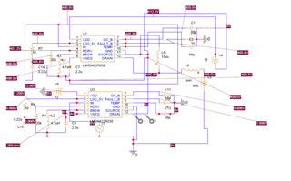
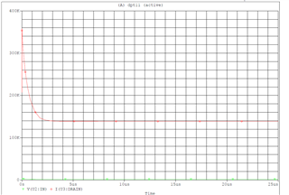
      I have attached my schematic and the results for Vds and Ids for your reference. As per the LMG342xx motherboard schematic, I replicated the setup and added a 10-ohm resistor in series with the 0.22 µF capacitor at the LDO pin. Unfortunately, I still could not achieve the expected double pulse test results. Could you kindly review the setup and advise on any additional changes that might be needed?
    2. Slew Rate Reduction Using Bootstrap
      Regarding the approach of reducing the slew rate of the low-side device by turning on Q1 MOSFET with the fault signal of the top FET:
      • When the MOSFET turns on, the effective resistance at the RDRV pin decreases, which, in theory, could increase the slew rate again.
      • Could you please clarify how this method effectively reduces the slew rate, despite the observed change in effective resistance?
    3. Use of Digital Isolator for H-Bridge
      For the H-Bridge configuration, I intend to use the same digital isolator for the gate pulses of both top-side switches. Considering the different switched nodes of these devices, would this approach be feasible? If not, could you suggest an appropriate isolator configuration?

    Your guidance on these matters would be greatly appreciated. Please let me know if any additional information is required to assist in resolving these issues.

    Thanks and Best Regards

    B Raja Sekhar

  • Hi B Raja Sekhar,

    John will replay to you shortly.


    Best Regards,
    Madhur

  • Hi Raja, 

    1. Try connecting the LDO5V cap without any series resistor. If this does not work, try removing the high-side device and simply replace it with a diode rectifier. This will allow you to characterize the low-side device.

    2.   Per Figure 5-4, a lower resistance at the RDRV pin yields a faster slew rate. When Q1 turns on, there are two resistors in parallel that are seen by the RDRV pin - this produces a lower effective resistance value. 

    3. Yes, this approach is feasible. 

    Best Regards,

    John