This thread has been locked.

If you have a related question, please click the "Ask a related question" button in the top right corner. The newly created question will be automatically linked to this question.

TIDA-020047: Reference design kit stack up inconsistency

Part Number: TIDA-020047
Other Parts Discussed in Thread: AWR2243

Tool/software:

Hi All,
I am working on to create a custom PCB board containing two AWR2243s with an some additional logic with it. I am currently reviewing the TIDA-020047 reference design and have some questions about the stack-up and blind via selection.

1- I think, there is a inconsistency in the Gerber PDF file and layer stack up written in the Gerber layer GM12. In the gerber pdf layers are as follows

Top layer
SIG1
GND2
PWR1
PWR2
SIG2
GND3
Bottom Layer


GM12 layer states the stack up as follows. Which one is the correct one?
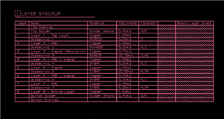
2-  When doing the via fence in the RF signals, Gerber shows 2 different via types used (100 um/150 um). 150 um vias are used for all  RF signals of the AWR2243 inputs and outputs whereas 100 um vias are near the antenna patterns. Is there a specific reason, this choice is selected? Can i used the same vias for every RF signals?

regards
Osman


  • Can you change it to the correct forum title which I did it wrongly.


    Regards

    Osman

  • Hi Osman, 

    1. Thanks for pointing out the inconsistency. In terms of layer stackup please follow the GM12 which follows as Top Layer, GND, Signal (sensitive), GND/Signal, Signal, PWR/Signal, GND and Bottom Layer. Can you also share the Gerber PDF that you are using so that I can double check? 

    2. In terms of via selection, please use the 2 different types of vias (100um/150 um) as the Gerber suggested. 

    Please let me know if you have any other questions. 

    Sincerely, 

    Ahanaf 

  • Hi Ahanaf,
    thanks for your response. 

    1- I am looking at the pdf file in the TIDA-020047 page. https://www.ti.com/lit/df/tidmb66/tidmb66.pdf?ts=1736200970621

    2- For the this question, Can you tell me the rationale behind this selection?

    Regards

    Osman

  • Hi Osman, 

    1. Please see the design guide for this design - https://www.ti.com/lit/ug/tiduf12/tiduf12.pdf?ts=1736267163643&ref_url=https%253A%252F%252Fwww.ti.com%252Ftool%252FTIDA-020047 Section 5.1.3.2 has the layer stackup which is same as the one in GM12.

    2. 100um vias are used for antenna purposes so I wouldn't recommend changing those vias. The other vias could be changed if needed. 

    Thanks, 

    Ahanaf 

  • Hi Ahanaf,

    Thank you for your response, which addressed most of my concerns about the stackup. However, after reviewing the document you referenced, I have one remaining question:

    Since all RF and antenna routing is on the top layer, would it be possible to use just a single layer of Rogers dielectric? Here's our current stackup:

    Layer 1 (Top): All RF and Antenna components
    Dielectric 1: Rogers 3003
    Layer 2 GND
    Dielectric 2 370HR
    Layer 3 Signal (Digital and low frequency only)
    Dielectric 3 370HR
    Layer 4 GND/Signal
    Dielectric 4 370HR
    Layer 5 Signal (Digital and low frequency only)
    Dielectric 5 370HR
    Layer 6 PWR/Signal
    Dielectric 6 370HR
    Layer 7 GND
    Dielectric 7 370HR
    Layer 8 (Bottom) Signal (Digital and low frequency only)


    Looking forward to your thoughts on this.

    Regards
    Osman
  • Hi Osman, 

    Here's my suggestions : 

    1. Layer 1 looks good with Rogers dielectric 

    2. Layer 2 GND can also be done with Rogers dielectric if needed and I would suggest you to use the Rogers dielectric as most of the RF signals are sensitive so it's best to follow the suggested layer stackup

    3. In the layout for this design, Layer 3 has a bunch of sensitive signals as well such as CSI. Which layer are you planning to route these sensitive signals? I highly recommend that layer to be done with Rogers dielectric

    And the rest of the layer stackup looks good. 

    Sincerely, 

    Ahanaf 

  • Hi Ahanaf,
    thanks for you suggestions. it helped alot. I need to change my previous stack up due to some other power constraints. Can you please take a look?

    Layer 1 (Top): All RF and Antenna components
    Dielectric 1: Rogers 3003
    Layer 2: GND
    Dielectric 2: RO4450F
    Layer 3: Signal (Digital and low frequency only)
    Dielectric 3: 370HR
    Layer 4: PWR
    Dielectric 4: 370HR
    Layer 5: PWR
    Dielectric 5: 370HR
    Layer 6: Signal (Digital and low frequency only)
    Dielectric 6: 370HR
    Layer 7: GND
    Dielectric 7: 370HR
    Layer 8 (Bottom): Signal (Digital CSI)

    I plan to route CSI signals on the bottom layer. Can you review the antenna performance impact? Also, how will the antenna performance be affected by signals and dielectrics from Dielectric 2 through Layer 8?

    Thanks
    Osman

  • Hi Osman, 

    I don't think routing CSI traces in the bottom layer would be good idea. As we prefer CSI routing to be sandwiched between two GND planes. If you plan to route them in the bottom layer then those CSI traces would only be referred to one GND plane which would be Layer 7. In terms of the antenna performance, I would suggest you to follow the design as you can't change anything about the antenna without repeating simulations that has been done during this design. And also as in your suggested layer stackup, you would have an extra FR board material which can result in an unacceptable loss for the 77GHz antenna. So, my suggestions would be please follow our recommended layer stackup. 

    Thanks, 

    Ahanaf